Control loops
I have been getting lots of questions from readers about
control
loops and loop stability, specially relative to switching power
supplies.
And now one of them asked outright that I write a web page about this
matter. Of course, control loops are amply and widely discussed in
electronic engineering books, but most of these books
rely heavily
on math, while most practical, hands-on electronicians seem to abhor
math more strongly than nature abhors vacuum!
So I will try to explain these matters in physical terms most
people
can visualize and understand. I will have to use some
mathematical concepts,
unfortunately, but far less than most textbooks do.
The concept of a control loop
It's all about having some device with an input and an output,
which
has a certain behaviour: Give it some input, and it will produce a
specific output that depends on this input in some way. And then, take
a sample of that output, compare it to what you want that device to do,
and calculate just the exact right input needed to force that device to
produce exactly the output you want. As simple as that.
Not simple enough? Well, look around you! The world is full of
control loops! For example, look at a car moving down the highway. The
car and its dynamic behavior is such a device. The input is the
position of the steering wheel, while the output is the direction the
car actually goes. The transfer function from input to output
is a
complicate one, not linear at all! It may be close to linear while the
car is moving slowly, without any wind. It will turn to whatever side
the steering wheel is turned. But when there is some side wind, the car
will tend to move sideways with the wind, and the steering wheel needs
to be turned slightly just to keep the car going straight! The same
happens when the road isn't perfectly level. When you drive over gravel
roads, the tires tend to slip significantly, and you need more rotation
of the steering wheel to produce a certain change of travel direction.
And as the car goes faster, things get really weird! In a turn at high
speed, the car might follow the steering wheel input up to a certain
amount of rotation, and then suddenly the tires lose grip, and the car
simply stops following steering wheel input! At that point, a totally
different strategy is needed to recover control, like moving the
steering wheel in the opposite direction, until control is re-gained ,
and then moving it more moderately.
With the above, it's clear that to make a car go straight, it
isn't
sufficient to tie the steering wheel in a fixed position. Instead, some
feedback is needed, that closes the loop. This feedback usually these
days is still a human being, sitting behind that steering wheel. It
senses what the car is doing, mainly through its eyes, but an
experienced
driver also feels what the car is doing, through, well, the part of his
body he is sitting on. He processes all the information, and constantly
makes little corrections to the steering wheel position. If this human
feedback system is working properly, the car stays well centered on the
lane, and follows all turns. If the human feedback system is still in
the learning phase, and thus is too slow in processing the
sensed
information, the car will likely go in slalom lines, but still stay on
the road, hopefully. And if the human feedback system is processing the
information far slower than normal, for example because of having
ingested a bottle of vodka, the usual outcome is that the car ends up
off the
road, against a tree, lightpole, or stuck in a building.
This teaches you that control loops need to be fast enough for
the
process they are controlling. Remember this. As a circuit designer,
your task is designing control loops that don't behave like they
have drunk vodka. Or at least not an entire bottle!
In electronics, control loops are everywhere. Every audio
amplifier
that uses negative feedback has such a control loop.
Regulated
power supplies are important examples, as are the position control
systems for a robot, the autopilot of an aircraft, or the trajectory
control system of a rocket launching a satellite into a precise orbit.
A PLL is basically a beautiful control loop, regardless of whether we
are talking about a simple PLL to decode an FM signal, or a PLL
frequency synthesizer. Industrial process controllers are basically
control loops on steroids, while a humble operational
amplifier is
normally also operated that way.
Characterizing the power section
The first thing we need to know, to design a control loop, is exactly
how the device we want to control behaves! And that's very often far
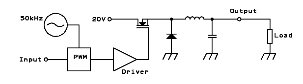
harder than it initially seems. Let's consider the following basic
switching voltage regulator, a simple buck circuit whose duty
is
to keep the ouput voltage constant, at, say, 12V:
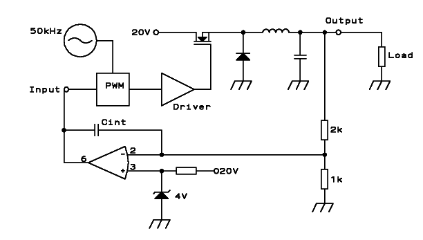
We have an oscillator that runs at 50kHz, feeding a Pulse Width
Modulator, which produces a 50kHz square wave output with a duty cycle
proportional to the input voltage. This wave is used to control a power
MOSFET, through a driver circuit. The MOSFET switches on and off,
applying 20V from the primary supply to the ouput filter when it is on,
and leaving that output filter floating when it is off.
Up to this point the behavior is simple. But what the filter does is
not very
simple at all! To simplify it, for a first approach, I will assume that
the load resistance is inside the range that will result
in continuous mode operation. This means that the current in
the
inductor never completely stops, but only fluctuates. Further down I
will add
what happens when this is not the case.
Whenever the MOSFET is off, the inductor
current can only flow through the diode. So, in continuous mode the
voltage at the node of
the MOSFET, inductor and diode will be about -0.7V (one diode drop)
whenever the MOSFET is off, and of course it will be very close to 20V
when the MOSFET is on. This gives us a square wave at this junction,
that has the same duty cycle as the one coming from the PWM, only
at other voltage levels.
If you look at this variable duty cycle square wave on a
spectrum
analyzer, you will see that it has (of course!) strong
contents at
50kHz and its harmonics, but also has a DC component and lower
frequencies. The DC and low frequencies present are an amplified copy
of the signal presented to the PWM's input!
The inductor, capacitor, together with the load resistance,
form a low pass filter. This filter does two things:
- It passes DC and low frequency components, while increasingly
attenuating higher ones. Normally it's designed for a cut-off frequency
much lower than the oscillator frequency, at least in a 1:10
ratio. So it will block the 50kHz signals reasonably well, and
its
harmonics even better, while passing the amplified copy of the PWM's
input signal to the output.
- It will affect the phase of all AC components passing through it.
While the effect on low frequency components is very small, even
negligible, the effect on high frequencies (50kHz, for example) is
dramatic, approaching a complete phase reversal! That means,
simply, that while the MOSFET is switching on, and the voltage at the
input of the filter is going up, the voltage at the filter's output
will be
going down!
It's a good idea to visualize the behavior of such a filter by means of
a pair of graphs, one showing the gain (or attenuation)
relative to frequency, the other showing the phase shift between input
and output:
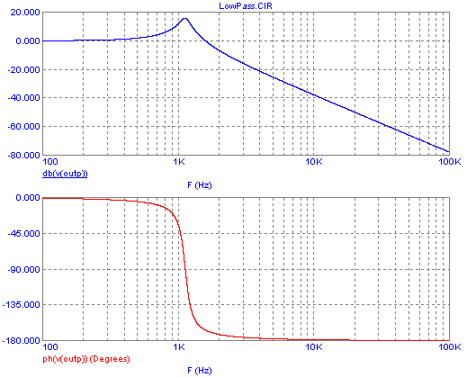
Such a pair of graphs is called a Bode plot. To design control
loops, you need to understand Bode plots, think in Bode plots, sweat
Bode plots, even dream of Bode plots!
So, let's start understanding this one. It's about a low pass
filter
having a cutoff frequency slightly above 1kHz, and loaded by resistor
of a moderate value, like an actual power supply might work. I only
cheated a little bit, and simulated perfect components, rather
than the real-world, lossy components we can buy! More about that later.
As you can see, at low frequencies up to a few hundred Hertz
this
filter does essentially nothing: The gain is zero dB, and the phase
shift is essentially zero too, meaning that the output of the filter is
identical to the input. That's entirely logical, considering that the
reactance of the inductor is negligibly small at these frequencies, so
that it essentially short-circuits the output to the input.
But as we approach the resonant frequency, things take a
rather
dramatic turn: The filter starts showing some voltage gain, up to about
17dB in this case, at its exact resonance. In the same frequency range
around resonance, the phase of the output changes dramatically,
reaching 90° phase lag at the exact resonant frequency, and then
approaching 180° lag at only slightly higher frequencies.
At even higher frequencies, well above the filter's resonance, we get a
steady behavior again, with a constant 180° phase lag, and a
negative "gain", or rather an attenuation, that grows at a steady rate
of 40dB per frequency decade.
Why precisely 40dB per decade? This number, that looks like cookbook
material, really comes from a very simple fact: The reactance
of
an inductor rises proportionally to the frequency, while the reactance
of a capacitor falls in inverse proportion to it. So, if we increase
the frequency tenfold, the inductor passes only 1/10th as much current,
and with the capacitor having only 1/10th its previous reactance, it
causes just 1/100th of the original voltage drop. As a result, for ten
times higher frequency, there is a hundred times less output. And a
voltage ratio of 100 times happens to be 40dB.
Closing the loop
To turn the open-ended circuit shown above into a
true loop,
you have to take a sample from the output, and process it to obtain a
suitable input signal that you can feed into the input. Designing the
circuit that does this is the
single most feared task many electronic designers have
to face! The evil devil of loop instability, often leading to seemingly
unstoppable self-oscillation, follows these poor fellows into their
sweetest dreams, turning them into churning nightmares!
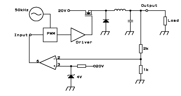
In a circuit like this voltage regulator, the first thing we need to do
is find out where we are standing, that is, what the present absolute
output voltage is! For this we need a voltage reference, and a
comparator of some sort. The voltage reference can be obtained from a
Zener diode with biasing resistor, but much better accuracy is obtained
from integrated circuits optimized as voltage references. And the
comparator can be implemented with a single transistor, or a pair of
them to cancel out their temperature dependency, but it's far more
common to use an operational amplifier for that task. From a very
simplistic point of view, we could end up with a circuit like
this:
The fundamental operation of this feedback system is simple: The 2k/1k
voltage divider produces a sample of the output voltage, being one
third as large in this case. For a 12V output, this would be 4V.
A Zener
diode is used to provide a 4V reference, and an op amp compares the
reference to the output voltage sample, and hugely amplifies the
difference between them. This amplified error signal is put into the
PWM. And then we hold all thumbs that it will work! The idea is that if
the output voltage gets a little too low, the op amp's output will get
much higher, this will increase the pulse width, thus raising the
output voltage and correcting the error.
But it won't work. At least not very well! Most likely the entire
loop will self-oscillate in a horrible way! Let's see why.
Stability criteria, phase margin, gain margin, and other
buzzwords
Any loop, like the one shown here, has the potential to oscillate, by
taking a signal from the output, putting it into the input, from there
to the output, and on, and on, and on... Whether it will actually
oscillate, or will be stable, can be defined in a very simple way:
- If there is any frequency at which the total loop gain is
exactly unity (0dB), and the total phase shift around the loop is
exactly zero, or 360°, or any multiple of that, the circuit will be
unstable. That means it will oscillate.
- If the above is not the case, but there is any frequency at which the
gain is higher than unity, and the phase shift is like above, then the
circuit will be "conditionally stable". That means, it will not
oscillate while these conditions are maintained. The problem is that
any momentary saturation condition of any part of the loop reduces the
average gain,
so that in practice such a circuit will typically at least momentarily
meet the conditions for instability, and will start oscillating. Once
it starts oscillating, the oscillation by itself keeps driving the
circuit into periodic saturation, self-adjusting the loop gain to that
sweet
value of unity, and thus maintaining the oscillation. So, for practical
purposes, a "conditionally stable" loop is an unstable one.
- If none of the above conditions are met, meaning that at each
frequency either the gain is less than unity, or the phase shift is
not 0°, 360°, nor any multiple of that, or both, the loop will be
stable.
So, to analyze whether our circuit is stable, we need to draw the Bode
plot for the entire loop. This is easier said than done!
We can start anywhere in the loop. Since we already have a Bode plot
for the low pass filter, let's start from there. The next element in
the loop is the resistive divider. It doesn't affect the phase of any
signals, and it divides everything by 3. That means a constant gain of
-9.5dB at any frequency, and zero phase shift. That's a Bode plot so
simple that I won't bother generating it. Combining this Bode plot to
that
of the low pass filter, the result is a new Bode plot for both
sections, that looks just the same as the Bode plot for the filter,
only that it has the entire gain curve shifted 9.5dB down.
The next part of the loop is the op amp. The voltage reference
connected to it only affects the DC response, and since
self-oscillation at DC is impossible, we don't need to bother about the
reference. But the op amp has a very characteristic Bode plot, which we
do need to consider. Here is a Bode plot for a typical, modest
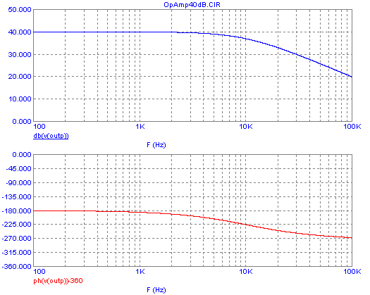
performance op amp:
Several things stand out here: Its very high gain at very low
frequencies;
the almost uniform gain drop-off throughout the higher spectrum, at
-20dB per
decade; and its phase shift, which starts from -180° at very low
frequencies, because I'm modeling an inverting amplifier,
and then soon shifts by another 90°, completing that shift roughly by
1kHz! In the gain plot we can see two clearly distinct
frequency ranges of operation:
The very low frequencies up to about 100Hz, where the gain is very
high and constant, and the higher frequency range above 100Hz,
in which the gain
drops at a steady 20dB per decade. Now if we take into account the
phase plot too, we need to consider the op amp as having three distinct
frequency ranges: The low range with constant high gain and constant
-180° phase, up to 10Hz; the high range, with downsloping gain and
constant -270° phase, from 1kHz up; and the transition range, from 10Hz
to 1kHz, in which the gain changes rather briskly from flat to
downsloping, while the phase changes much more gradually from -180° to
-270°.
These curves are typical for any op amp, although the very low
frequency gain, and the transition frequency, depend on the specific op
amp.
Note that when talking about phase shift, 180° is the same as -180°,
90° is the same as -270°, and so on. You should also be warned that
most other authors, when discussing these matters, don't mention the
fact that error amplifiers are usually inverting amplifiers, and so
they would talk about a phase shift changing from 0° to -90° in this
case. It doesn't matter which method you use, as long as you are aware
that in any negative feedback system, like control loops are, there is
always a phase inversion, meaning that the reference of all things is a
-180° phase shift!
In the same breadth I should mention that most authors draw their Bode
plots as straight lines with sharp corners, that approximate the actual
softly curving lines.In my opinion, that's a dangerous practice,
because the actual traces can deviate by several dB and tens of degrees
from the straight
line drawings, misleading a designer into making an unstable circuit!
For this reason I'm using the actual, curvaceous traces in my Bode
plots. They are more beautiful too!
The output of our op amp goes to the PWM. We need to come up with a
Bode plot for the entire cell consisting of this PWM, driver, and
MOSFET. Assuming that we are using the PWM included in typical power
supply control ICs, the input range to the PWM will be typically
something like 1 to 3V, to produce an output from zero to 100% duty
cycle (or close enough to that). The average voltage after the MOSFET
will be this same percentage of the 20V input! So, at 20V input, and
given the total 2V control range, this cell of our regulator has a
voltage gain of 10, which is
20dB.
This holds true from DC to the highest frequencies that still
allow
proper PWM operation, that is, frequencies that are much lower than out
50kHz clock oscillator. When our signal frequency comes into the same
range of the clock frequency, better forget it, because all sorts of
weird things happen!
You might think, at first, that a PWM causes no phase lag. But... it
does! The problem is of a statistical nature: Whenever the input
voltage to the PWM changes, the PWM cannot transfer this change to the
output any faster than the individual pulses happen. So, it causes an
input-to-output delay that averages one half pulse, which would be 10µs
in our example. At low frequencies a delay of 10µs means a negligible
phase delay. For example at 100Hz a cycle takes 10ms, so a delay of
10µs is about one third of one degree phase lag. But at the higher
frequencies the phase lag becomes progressively larger.
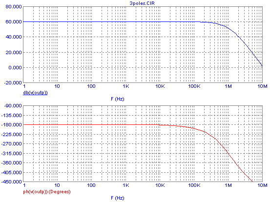
Now we have characterized all elements of the loop, and need to combine
all those Bode plots. The result is something like this:
It's not totally accurate because I was too lazy to model it
in
full, and what's more worrying, because this circuit simulator produces
nonsensical output as soon as the DC gain exceeds 80dB! That forced me
to tweak some things, resulting in a gain curve about 15dB lower than
the real thing, but it's close enough for this crude analysis. The only
facts
you need to
see right now are these: At low frequencies the loop has a very high
gain, which is highly desirable to achieve a precise output voltage,
and the phase shift is close enough to -180° so that we can consider
this to be valid, true, negative feedback. But around 700Hz
the
phase lag quickly grows, and by the resonant frequency of the filter,
around 1.2kHz, it reaches -360°! That means, in addition to the desired
inverting action of the op amp, there is an additional, full 180° phase
lag, coming from the low pass filter, making a total lag of 360°. Now
remember the stability criteria: Where the phase
lag is 0° (or 360°, or a multiple of that), the gain is not allowed to
be 1 or higher. But our circuit has a whopping gain of over 80dB at
this frequency! So it is "conditionally stable" only, which means that
in practice it will be unstable!
The actual behavior of this circuit would be that of a simple
on/off
controlled loop: At first the op amp would drive the PWM to 100% duty
cycle, so that the MOSFET would be continuously on. The output voltage
would rise at a rate determined by the low pass filter, and when it
crosses the 12V barrier, the opamp would ramp down and drive the PWM
into its zero duty cycle range. So the MOSFET would switch off for a
long time, after having done only a few pulses of decreasing width at
50kHz. It would stay off
for a long time, while the inductor keeps delivering current to the
capacitor, and the output voltage keeps rising for a while, until
running out of juice. At that time the voltage starts dropping, and
when it crosses the 12V barrier again, downward, the op amp would ramp
up again, the PWM would again go to 100% duty cycle, and so on.
In short, the circuit would oscillate at the low pass
filter's
resonant frequency,
and the 50kHz oscillator and PWM would be basically defeated! At the
output we would get a 12V average voltage, so the circuit sort of works
- but there would be a large 1.2kHz ripple on it! And the
current
in the coil and transistor would reach dangerous levels. All this would
make
the circuit unusable.
We clearly need to get rid of the excessive gain at the
critical
frequency where the phase lag reaches zero. An obvious thought is to
add gain controlling resistors to the op amp. But this isn't a good
solution! For example, see what happens if we reduce the gain of the op
amp to just 10 (20dB):
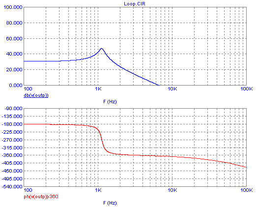
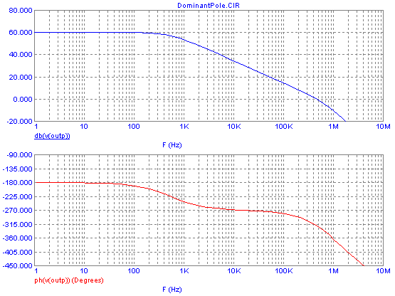
What we have now is basically the filter's phase response up to several
kilohertz, because the op amp has a pretty clean 180° phase inversion
up to that frequency, at this low gain setting. The op amp's phase
delay comes in only from 10kHz upwards, bending the phase curve down.
That's good. But we get a total loop gain at low frequencies
that
is only about 30dB. This is given by the 20dB gain of the PWM and power
stage, the zero dB of the low pass filter, the almost 10dB attenuation
of the resistive divider, and the 20dB gain of the op amp. This isn't a
brilliant amount of low frequency gain to have! Any disturbance, for
example 100Hz ripple riding on our 20V primary supply, will get through
to the ouput, with only 30dB attenuation. That's poor performance! And
even worse: At the frequency where the phase lag crosses zero, we still
have several dB of gain, so the circuit would still be
unstable!!!
Of course we could achieve stability by brute force, simply by lowering
the op amp gain enough. But by then we would have very little
regulating action left, rendering the whole circuit pointless!
It's pretty clear what we could use: High gain at low frequencies, but
rolling off fast enough, along with a controlled phase behaviour, so
that we meet the stability criteria while at the same time providing
good regulation!
To do this, we need to know just how low the gain needs to be, at the
phase crossover frequency. This is where the concepts of phase margin
and gain margin come in. Gain margin is simply how much the loop
gain is below unity at the exact frequency where the phase
response
first crosses zero. And phase margin is how many degrees away
from zero (or 360°, or -360°) the
phase is, at the exact frequency where the gain is unity (0dB).
The Bode plot above shows that the gain margin we obtain is about
-13dB, since the gain is about +13dB at the phase zero crossing. And
the phase margin in that plot is roughly -8°. Instead the values that
usually are considered desirable are a phase margin of about 45 to 60°,
and a gain margin of about 6 to 10dB. If a circuit operates under many
different conditions, these criteria should be met at the worst of all
operating conditions.
Clearly we aren't there yet!
Shaping the loop response, poles and zeroes, and the
PID control function
Now it's about high time to learn, if you haven't yet done so, how an
op amp behaves when you connect different stuff to it. Because we need
this tool to shape the response of our error amplifier, to achive good
regulation along with full stability.
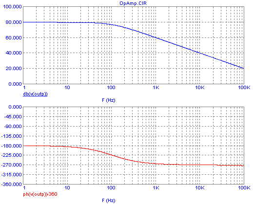
You already saw the Bode plot resulting from a naked op amp: Very high
gain at very low frequency, tapering off smoothly at 20dB per decade,
while the phase response starts at the desired value (180° in an
inverting amplifier) at those very low frequencies, and then soon
adds 90° of lag. Now let's see what happens when we add a
simple
resistive feedback network to the very same op amp, like this,
a
40dB gain inverting amplifier:
We get the following Bode plot:
See how the same op amp that had such a crummy response when left
without any feedback, now has a nice, very stable gain up to several
kHz, and at the same time its phase
delay gets significant only above 3kHz too! This is called a
proportional amplifier, because it amplifies all frequencies by the
same proportion, up to a limit given by the op amp's characteristics.
Above
that range, the op amp internally limits the frequency
response
and causes a phase lag.
Note that what the resistive feedback does, relative to the bare bones
op amp, is simply pushing down the gain in the flat response area,
without changing the position of the sloping gain line. This moves the
intersection of the two lines (or rather, the bend) up in the spectrum,
and with it goes the 90° phase delay.
For a given op amp, the lower the gain you program it for, the wider
will be its flat gain, no-lag bandwidth.
But very often we want an error amplifier to have far more gain at low
frequencies than at high ones, even within our frequency range of
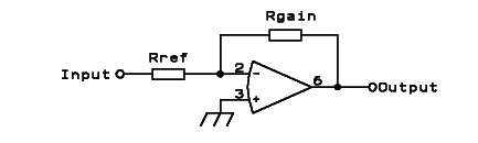
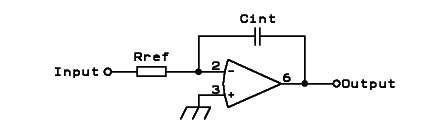
interest. This is done using capacitive feedback:
This circuit is called an integrator, because its output is the
integral of its input. Put a voltage step in, and you get a ramp out.
Put a square wave in, and you get a triangle wave out. Put
a sine
in, and you get a cosine out - or the other way around, I
don't
remember, being mathematically challenged myself... To non-mathematical
electronicians, anyway, it's the same sine, shifted 90° back in phase.
Its Bode plot is rather boring:
But such boring Bode plots, with very straight lines, are
often the
most useful! You can see that throughout the frequency range in which
it functions as an integrator, it has a gain sloping down at a constant
20dB per decade, and a constant phase shift of -90° relative to the
standard -180° of any inverting amplifier.
The lower limit of this behavior is given by the finite DC
gain of
any op amp, which turns it into a proportional amplifier in the very
low frequency range, tending to very high, constant gain
there,
and only
the normal 180° shift. Just the beginning of this is visible in this
plot, that starts from 100Hz. And the upper limit of the clean
behavior is
given by other internal effects of the op amp, adding an
additional phase delay, but at frequencies far above than our range of
interest.
So, what the capacitive feedback does, relative to the bare-bones op
amp, is basically shifting the sloping part of its gain curve
down, without affecting the flat, low frequency line. This moves the
intersection frequency down, out of the graph in this case. It's easy
to make an integrator, with practical component values, that has an
intersection frequency as low as 0.01Hz!
At DC, the gain of an integrator is always the op amp's open loop gain,
typically 80 to 100dB.
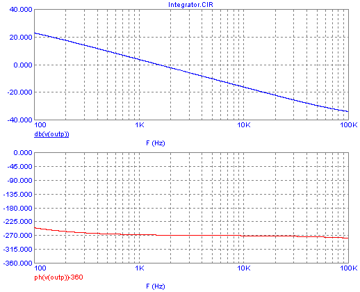
Of course we can also build the opposite circuit, one whose
gain increases with frequency:
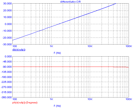
This is called a differentiator, because its output is the derivative
of the input: A ramp on the input produces a step on the output, a
triangle at the input gives a square at the output, and a cosine at the
input gives a sine at the output - or the rounder way another, because
I'm still mathematically challenged! Anyway, it shifts sine waves in
the opposite direction as an integrator does.
And its Bode plot:
You can see the steadily rising gain, at 20dB per decade, until
reaching a limit given by the op amp's characteristics. The phase shift
is -90°, which is a positive shift of 90° relative to the -180°
of any inverting amplifier. But the imperfections of a practical op
amp, built in intentionally (and necessarily) in the form of a
compensation capacitance, start causing an increasing phase lag from a
few kHz up.
Since this plot looks too crooked, I ran the simulation again, using a
better op amp. The difference is impressive! I kept the same scaling,
to make it obvious:
Here we have a clean differentiator! Keep this in mind: When
you
are caring only about low frequencies, cheap op amps like the 741, 358,
or 324 are fine. But when you need an op amp to perform cleanly at
somewhat higher frequencies, be so good and pay a little more for a
better one! The op amp used for the crooked differentiator is a 741,
and some of the op amps inside power supply control ICs are even worse!
Instead the one used for this last Bode plot is an LF400.
The gain of the differentiator keeps decreasing toward lower
frequencies, so that at DC it reaches infinite attenuation. That means
its output doesn't react at all to any DC voltage at its input.
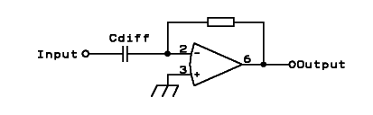
We can combine the functions of proportional, integrating,
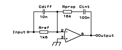
and differentiating amplifiers in a single circuit. For example, this
circuit has all three of them:
At DC, both capacitors behave as open circuits, so that the amplifier
has the op amp's full open loop gain. In the low frequency range, the
reactance of the integrator capacitor is high relative to the
proportional gain resistor, so it dominates the series pair. At the
same time, the differentiator capacitance also has a high reactance
compared to the reference resistor, so that in this parallel pair, the
resistor dominates. The result is that in low frequency range the
circuit operates as an integrator.
In the middle frequency range, Cdiff's reactance is still large
compared to Rref, but Cint's reactance has become small compared to
Rprop. As a result, both resistors dominate, and the capacitors are
ineffective. As a result, in this middle frequency range the circuit
operates as a proportional amplifier.
And in the high frequency range - you guessed it - both capacitors'
reactances are small compared to their companion resistors, so that in
the input parallel group the capacitor dominates, and in the feedback
series group the resistor dominates. As a result, the circuit operates
as an differentiator in this high frequency range.
The whole affair is called a PID controller, and you will hear this
buzzword mentioned very often in the context of control theory. PID, of
course, stands for "proportional, integral, derivative". PID
controllers are used very, very often. And I do mean that!
Other authors call it a lag-lead circuit, because it offers
phase lag in some frequency range, and phase lead in another.
To an audio person, this exact same circuit goes under the name of
"bathtub equalizer". Just look at the gain curve below, and you know
why! Lots of bass emphasis, some treble emphasis, with a depressed
midrange. It's a common way to make a cheap ghettoblaster
sound
"like a big rig", at least to the ears of non-discerning listeners. And
this brings us to its Bode plot:
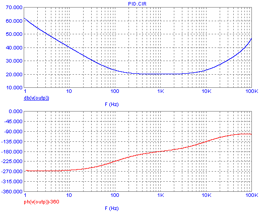
As you can see, in the low frequency range we have an integrating
behavior, characterized by a -20dB/decade gain slope and a phase of
-270°. In the middle frequency range we have a flat, low gain, the
phase being nominally the -180° of any inverting amplifier. And in the
high frequency range, the differentiator kicks in, with the gain
sloping up at 20dB/decade, and the phase being 90° advanced relative to
the -180° of the inverting amplifier, that is, -90°. This holds true up
to a frequency where the performance of the specific op amp starts to
fall apart.
It's high time now to introduce two more of our friends, poles and
zeroes. A
"pole" is a fancy name given to bending the gain curve down,
for example from flat to -20dB/decade, or from -20 to -40dB/ decade.
Any pole also causes the phase to shift 90° more negative. A "zero" is
an equally fancy name given to the opposite effect, that is, the gain
curve bending up by a step of 20dB/decade, and the phase shifting 90°
more positive.
In the Bode plot above, we can see two zeroes, one located at
100Hz, the other at 10kHz. The circuit actually also has at least two
poles, but they fall outside the frequency range of this plot. One
happens at a very low frequency, where the integrator's gain curve
intercepts the open loop gain of the op amp, probably around 80 or 90dB
gain, and close to one tenth of a Hertz! The other
one, for
this op amp under these conditions, probably happens at a few
hundred kHz. The very beginning of it is visible in the plotted phase
curve.
At the exact frequency of a pole or a zero, the gain is 3dB
off
the "straight line" value obtained by drawing best-fitting straights,
and the phase shift is precisely 45° off the starting value.
This
can be seen very nicely in the plot above.
The design of such a PID amplifier is pretty simple: You first pick a
convenient value for the reference resistor. Then you calculate the
proportional gain resistor to give it the proper mid-frequency gain. If
you want a gain
of ten (20dB), make it ten times as large as the reference resistor.
Then you place the two zeroes. The lower one is placed by calculating
the integrator capacitor value such that its reactance is equal to
Rprop at the desired lower zero frequency, 100Hz in this case. Then you
calculate the differentiator capacitance, such that its reactance is
the same value as the Rref at the desired upper zero frequency, 10kHz
in this case. Finally, if impractical or inconvenient component values
result, you can
scale all four values as you like, increasing the resistances in the
same proportion you decrease the capacitances. Ready!
Phew!
But now we have to put this knowledge to work for us. We still have a
task waiting: Designing a good, fast, stable feedback circuit for our
voltage regulator! We already tried using a simple proportional
amplifier, and found that if we reduce its gain enough to reach
stability, the gain at low frequencies is way too low, resulting in
very poor regulation. So, the next step is trying to use an integrator
instead, which is no more complex than the proportional amplifier. We
only need to replace the feedback resistor by a capacitor, like this:
But this time we will calculate the optimal value! And the logic goes
like this: Since our feedback amplifier is an integrator, it will have
-270° phase shift. So, at the frequency where the lowpass filter of the
power section provides another -90° phase shift, the total phase shift
will reach a full 360°, the condition for oscillation. At this
frequency, which is the filter's resonant frequency of 1.2kHz, we need
the total loop gain to be -6 to -10dB, to have adequate gain margin.
We saw way up in this page that at this frequency the low pass filter
has
17dB gain. The PWM and power stage, fed by 20V, provide 20dB gain. And
the 2k/1k voltage divider provides nearly 10dB of attenuation. So we
have slightly over 27dB of gain left, and we need -6dB or
lower,
which means that at 1.2kHz the error amplifier must provide -34dB of
"gain". 34dB is a voltage ratio of 50, meaning that the integrator
capacitor must have a reactance 50 times lower than the input
resistance to the amplifier, at 1.2kHz.
The effective input resistance, in this circuit, is given by the
parallel equivalent of the 2k and 1k resistors. This is 667Ω. So, the
capacitor needs to have a value of 10µF. If this value seems
impractically high for a nonpolarized capacitor, of course the values
can be scaled, for example you can use 1µF and replace the divider
resistors by 20k and 10k.
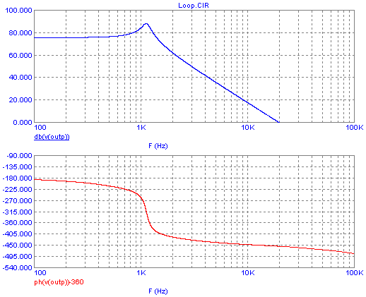
The Bode plot for the total loop, including this integrating error
amplifier, looks like this:
As you can see, at the frequency where the phase lag reaches 360°, the
gain is -7dB, satisfying the gain margin requirement for stability. And
where the gain becomes zero, at about 80Hz, the phase lag is 270°, so
the phase margin is 90°, which is plenty. This means that the loop will
be stable using this integrating error amplifier. But its low frequency
gain is still poor! Quite a lot better than that of a stable solution
based on a low gain proportional error amplifier, but still poor. For
example, if there is 100Hz hum on our 20V primary supply, the low pass
filter doesn't attenuate it at all, as it has 0dB gain there. And the
error amplifier has about -2dB gain at that frequency, and the voltage
divider has almost -10dB, so that the control circuit will do very
little to reduce the 100Hz hum. It will pass right through to the
output, making this a poor regulator!
We need something better. And we need to think a little, what we can do
to make it better. The problem is simple: The low pass filter provides
good attenuation of any unwanted ripple, only well above its resonant
frequency. So, at low and middle frequencies, through and somewhat
beyond the resonant frequency, only the feedback circuit can be used to
reduce any unwanted ripple, noise, and other crap. So, we absolutely
need a sufficiently high gain in the error amplifier, through and
beyond the
resonant frequency of the filter! But the filter introduces a nasty,
quite abrupt 180° phase change around its resonant frequency. This
shift goes from 0° at low frequencies, to -180° at high ones. So, the
best thing we can do, given that we can't eliminate the 180° phase
change, is move it up, so that the total loop phase response, instead
of being -180° to -360°, or worse yet, -270° to -540°, becomes -90° to
-270°! That range accomodates the low pass filter's phase change, and
it also satisfies the phase margin stability criteria, at any frequency!
The tool for achieving this goal is giving the error amplifier a
differentiating action, in the frequency range around the filter
resonance, and up to the frequency where the gain has dropped well
beyond unity. But we can't use a simple differentiator as an error
amplifier, because its response at DC would be none at all! And at low
frequencies it would be dismally low. So, we still need an integrator
to get enough low frequency and DC gain, but then we introduce a zero,
and another zero, both below the filter's resonant frequency. The first
zero compensates for the integrator's phase shift, bringing the error
amplifer's phase back up to -180°. And the second zero brings it
further up to -90 degrees, so that the entire loop phase response would
then start at -270°, move up to -180° and -90°, and then at the
filter's resonance move down again to -270°. Given these
phase shifts,
we can give the error amplifer any gain we want, and still get
stability! The only practical limit to gain is that at very high
frequencies some additional phase lags appear, in the op amp and
elsewhere,
so at those frequencies the gain must be low enough to maintain
stability. But at those high frequencies the low pass filter is highly
effective, so we don't need any error amplifier gain there.
Let's see how to implement this.
Let me start by telling you that the two zeroes might be placed on
different frequencies, or might be placed both on the same
frequency! This actually gives the best low frequency gain,
for a
given very high frequency zero gain crossing. Let's try it, using our
PID circuit. And let's try placing the zeroes on 500Hz, and see what
happens. This should be low enough to have them give a good phase boost
at 1200Hz, and at the same time high enough to avoid reducing the mid
frequency gain too much. Also let's make an integrator that provides a
gain of 40dB at 100Hz, to get reasonable ripple reduction.
Taking our PID circuit, and using our 667Ω equivalent input
resistance for Rref, we neet an integrator capacitor that has
66.7kΩ reactance at 100Hz, to give the 40dB of gain there. This is a
value of 24nF. Then we place one of the zeroes, by means
of Rprop,
which needs to have the same value as Cint's reactance is at 500Hz.
This is 13.3kΩ. And then we place the other zero at the same frequency.
For that we need a Cdiff that has 667Ω reactance at 500Hz.
This
is 477nF.
Here is a little quirk of my chosen voltage regulator circuit: Since I
used the 2k/1k voltage divider as input resistance for the error
amplifier, there isn't an obvious place to put Cdiff! So we place it in
parallel with the 2k resistor, but then it sees three times higher
voltage, so it has to be one third as large! As a result, we need a
159nF capacitor in parallel with the 2k resistor.
Of course in a practical circuit we would use the closest standard
values, such as a 22nF capacitor for Cint, a 13kΩ resistor for Rprop,
and a 160nF or even 150nF or 180nF capacitor for Rdiff.
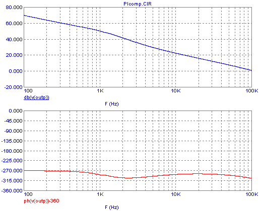
And the Bode plot for the entire loop now is:
As you can see, now the phase for the whole range from DC to over 10kHz
never gets closer than about 65° to the dangerous -360° limit. The
phase shift problem caused by the low pass filter has been removed!
Also the DC and low frequency gain is excellent, at medium frequencies
the gain is still plenty, and life is good - except that a new
resonance showed up at 20kHz! There the phase shift crosses the 360°
line, and the total loop gain there is still high, like 40dB! That
means: Oscillation!
I think that roughly at this time you start realizing that control loop
design isn't for the faint of heart, nor for people seeking instant
gratification!
Actually I'm not sure where this new resonance is coming from. It might
be a quirk of the simulator, rather than a real effect, or maybe it's
real indeed. In any case, it's happening at the frequency where the op
amp reaches its limit, and a downward gain slope begins due to the op
amp proper. Due to the differentiating function, and the relatively
high starting
gain at mid frequencies, at 20kHz the op amp is expected to deliver
close to 100dB gain, which it isn't capable of.
We could do two things: Either build the circuit for real, and try it,
or first roll off the gain at high frequencies, where we don't need
gain, really. The problem is that any gain roll-off at high frequencies
means inserting a pole, which in turn means shifting the phase response
90° down. And that would bring us into oscillation land right away! So
it looks like we need to sacrifice some overall gain.
I will try to do a few things: First, add a pole at 5kHz, by inserting
a 200Ω resistor in series with our 160nF Cdiff. This cancels the
differentiating action from 5kHz up. See what happens:
Much, much nicer! The resonance peak and its associated
sudden
180° phase shift have gone away. But the -360° crossing happens at a
frequency where we still have a positive loop gain. So we still get
oscillation!
At this point, the best course of action seems reducing the overall
gain. Let's try that. We have -360° phase at about 15kHz, where the
gain is around 7dB. If we reduce the gain by, say 15dB, we should get
stability. 15dB is a voltage ratio of 5.6. Let's round it to 6, since
I'm tired at this time of the night, having spent all day writing this
page. So we increase Cint to 144nF and
reduce Rprop to 2.2kΩ. The result:
Success! Now at the -360° phase point, we have -8dB gain, enough to
satisfy the gain margin criterion. But... ouch! The phase
margin
criterion is not satisfied! At 0dB gain, we have very little phase
margin!
Do you like this game? It can be addictive! Maybe after another 10
rounds we solve the problem! ;-)
Math gurus say that they can start from the power circuit parameters,
fill roughly 25 sheets of paper with integral calculus, enormous
intimidating matrixes, a lot of small scribbling along the edges, and
then come forward
with the perfect component values for the error amplifier. The only
problem is that in all instances I have seen them trying to actually do
it, their circuits didn't work as calculated, and had to be tweaked
anyway!
At this point, we could simply solve the problem by reducing the gain
even further. You see, this is like a mantra: If it oscillates, reduce the gain! We
would need to place the -6dB gain point pretty much at
2kHz or so, to just meet the phase margin requirement. But then we are
back to having insufficient low and mid frequency gain! What we need is
either a steeper gain roll-off without the associated phase lag, or
else keeping the phase high enough up to a high frequency, where the
low pass filter cuts the gain enough - but that phase boost would have
to come without any additional high frequency gain! Both are wishful
thinking.
It seems that I cannot come up with a really good, fast, high gain,
reasonably simple, and
unconditionally stable control circuit for this simple voltage
regulator!!! About the best I can do is slightly shift
down the
pole I had placed at 5kHz, and add an additional pole at a somewhat
higher frequency, by means of adding a capacitor in parallel with
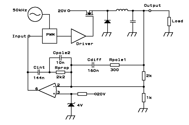
Rprop. This is a so-called "Type-III" compensation circuit.
I think I'm right on the money if I assume that by now you are just a
little bit
lost about the exact circuit configuration I'm talking about, so here
is
the schematic of the final circuit. It still has the PWM and
driver shown only as blocks, but that shouldn't be a problem.
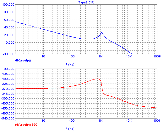
And this is the full-loop Bode plot it provides:
Looking at it closely, you can see that the gain margin is about the
required minimum 6dB, while the phase margin is a bit tight, barely
20°. So this circuit will have a tendency to ring at about 3kHz, but it
should not self-oscillate. At the same time, its low frequency gain is
high, so the voltage regulation accuracy will be good. In the mid
frequency range, the gain is mediocre to poor, so any ripple on the
primary supply will get through to the output, with a significant
amplitude. Sorry, friends! It's all I can do.
The power of imperfection
Now let me break some bitter news to you: All of our careful tweaking
of this error amplifier was complete nonsense, and utterly useless,
because the power circuit we were trying to control can only exist in
Simulatorland! Because it uses perfect, lossless components. But the
real world just isn't nearly as simple! Real components are imperfect.
Capacitors have some Equivalent Series Resistance, which isn't
negligible in circuits like this. Inductors have a lot of ESR too, and
what's worse, the ESR changes with frequency! At DC it's just the
wire's resistance, but at several kHz and higher an additional
resistance shows up, which is caused by loss in the magnetic core. And
what's even harder to manage is that inductors are quite non-linear
with current! Not only their ESR changes with current, their inductance
also does so, and quite dramatically if you get close to the saturation
zone!
The consequences of this are two: The simple power circuit we were
trying to compensate just doesn't exist in the real world, and what's
worse for the virtual electronician, it's extremely hard to correctly
simulate such a circuit in software! Regardless of how much effort you
invest in getting your simulation right, the real circuit will still
behave differently. You can only get close with the simulation, and how
close you get depends quite a lot on sheer luck, because there are
always some things you don't know about your real circuit. The level of
agreement between
electronic circuit simulators and the actual circuits is about as good
as that of a 5-day weather forecast with the actual weather! To say it
bluntly: Circuit simulators are liars in the same
class as
meteorologists! Both have the best intentions of getting it right - and
both miss the mark by a wide margin!
I tend to use simulators only for relatively simple cases, and when I
know well enough what should happen, to make a reasonable sanity check
of the simulator's output. For this article I'm using Micro-Cap, simply
because it allows me to create nice-looking Bode plots. But when I have
to design an actual control loop, I first measure the behavior of the
actual, real, physical circuit.
Anyway, for now let's continue using the simulator, but let's simulate
at least some better approximations to the actual behavior of our
circuit! It's very important to do so, because the imperfections of
electronic components are not always a problem. In some specific cases,
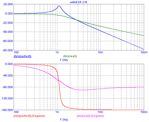
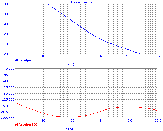
like the one on hand, they can play in our favor! Here is the Bode plot
of our low pass filter, in two versions: The blue gain curve and red
phase curve are the exact same as those in the very first Bode plot on
this long web page, showing the response of an LC low pass
filter
with perfect, lossless components. By the way, the values are 20µH and
1mF (old fashioned people write that as 1000µF), and a 1Ω load. The
green gain curve and pink phase curve are the very same filter, but
adding the ESR for each part. I added 0.05Ω ESR to the capacitor, which
should be quite realistic, and 0.16Ω ESR to the inductor, which implies
an inductor Q factor of 50 at the resonant frequency, which is also
quite realistic for the type of inductors commonly used in switching
power supplies. Now look what happened:
As you can easily see, the resonance peak of the filter has simply
disappeared, and the worst phase lag caused by the real world filter is
only about 100°, compared to the 180° of the theoretical, perfect
filter! And each of these two differences helps us a whole lot in
designing an error amplifier that provides enough mid-frequency gain
along with good
stability!
This subject is important enough to analyze it in more detail, from DC
to high frequencies: At DC and up to about 100Hz, the parasitic
resistances have very little effect. Basically the gain curve is a tad
below 0dB, because the ESR of the inductor forms a voltage divider with
the load resistor. But at all higher frequencies the ESRs are
important. The 20µH inductor has a reactance equal to
its 0.16Ω ESR at 1273Hz, so
that upwards from this frequency the inductance starts to
dominate. As we go below this frequency, the inductor actually tends to
behave ever more as a 0.16Ω resistor! And the 1mF capacitor
has a reactance equal to its 0.05Ω ESR at 3183Hz, so it's mainly
capacitive only well
below this frequency, and instead behaves as a 0.05Ω resistor well
above it! And that explains what happens:
At low frequencies we don't have significant inductance, and instead we
have an RC low pass filter: 0.16Ω in series, and 1mF to ground. The
pole frequency of this combination is 995Hz, and explains the first
half of the phase response bend, and the inflection from constant gain
to a -20dB/decade gain slope. At high frequencies instead the
inductance dominates over its ESR, but the capacitor has become a
resistor, so we have an LR low pass filter in that range! This explains
why that range also has only a -20dB/decade gain slope, and only -90°
phase shift. Only around 3kHz we have a mix of inductance, capacitance,
and both resistances, so there we get slightly more phase lag than 90°,
while the increase in the gain slope is barely noticeable, but present.
At the "resonant" frequency neither the inductor nor the capacitor are
pure enough to cause any noticeable resonance effects!
If the ratios of ESR to inductance and capacitance were slightly
different, putting the inductor's pole frequency right on the
capacitor's zero frequency, we would get a clean
first
order response from this filter, meaning a very smooth -20dB/decade
slope and a precise -90° phase lag, without any overshoot! The inductor
would
basically start filtering at a frequency where the capacitor stops
doing so. The problem in doing this in practice lies in the poorly
defined ESR of capacitors. Manufacturers will guarantee a certain
maximum ESR, but not a minimum, and then the ESR changes a lot during
the life of the equipment, going up as the capacitor ages. So it's
always unsafe to rely on en electrolytic capacitor's ESR to
stabilize a loop,
but it's what almost everyone does in this trade!
What can be done, to remove this uncertainty, is using very low ESR
capacitors, such as plastic film or multilayer ceramic capacitors
instead of electrolytics, and then deliberately adding some series
resistance. Very often this can be done simply by using narrow, long
circuit board traces! Where that introduces too much inductance, a very
low value resistor can be used. And don't shudder thinking of a giant
1000µF ceramic capacitor! Modern high frequency switching systems often
need suprisingly low values of capacitance.
Let's get back to our humble voltage regulator. It's time to cook up a
new error amplifier for it,
now that we have a more realistic Bode plot for the filter's behavior!
The logic will be this: The largest phase lag of the filter is 100°, at
3-5kHz. As long as the error amplifier doesn't introduce much
additional phase lag, the circuit will be stable! But a simple
integrator of course introduces 90° of lag, and that's not acceptable.
So the simplest error amplifier circuit we could try is one having a
single zero, behaving as an integrator at low frequencies, and as a
proportional amplifier at middle and high ones. That would be a PI
controller, or a pole-zero compensator, depending on the lingo you
speak. Pole-zero is because in addition to the zero you introduce
deliberately, there is the natural pole formed by the op amp running
out of open-loop gain at extremely low frequencies.
To have the error amplifier introduce little phase lag at 3kHz, we
need to place the zero well below that frequency. I will try 1kHz. And
then we have just one more decision to make: The overall gain. How much
we can use depends on the high frequency response of the op amp,
because as it runs out of bandwidth it will naturally turn into an
integrator, inserting a pole, causing a -90° phase shift, and at that
point the total loop gain needs to be low enough. Given that I'm using
a pretty good LF400 in my simulation, I will shoot for 40dB
proportional gain. This means:
From very low frequencies to about 1kHz the low pass filter has flat
response, while the error amplifier slopes down by 20dB/decade, from
the op amp's open loop gain to 40dB; while
from 1kHz upwards the low pass filter is the one that slopes down at
that 20dB/decade, while the error amplifier has constant gain! The
result
should be a nice smoothly sloping gain curve, along with an acceptable
phase response.
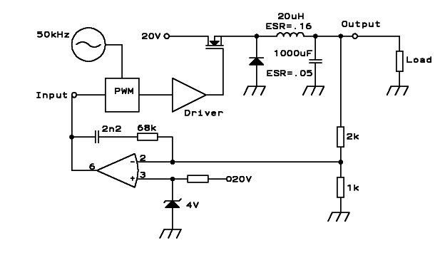
Given our 667Ω input resistance (from the 2k/1k divider), 40dB
proportional gain needs a 66.7kΩ resistor. Let's use a practical,
available 68K one. And to get a zero frequency of 1kHz, the integrating
capacitor needs to have that 66.7kΩ reactance at 1kHz; that's a 2.38nF
capacitor. Let's use a standard 2.2nF one. Our circuit ends up looking
like this:
And the Bode plot for the entire loop is:
It's pretty nice! The phase margin is around 55°, which is
fine.
The gain margin can't be seen in this plot, as the phase lag
of 360° occurs at a much higher frequency, but the shape of
the
curves seem to show that the gain margin will be ample. The gain at
100Hz (grid ripple frequency!) is 70dB, which will afford a very good
ripple rejection. DC gain is basically the op amp's open loop gain plus
20dB for the power circuit minus 10dB for the voltage divider, which
assures a very precise regulation (as long as our zener is good, that
is...). All is fine, and this circuit should work well. Do you agree?
In fact many switching regulators use simple PI error
amplifiers
like this one. It tends to work well in practice - thanks to filter
component imperfections!
If I needed to deliver a design from which a company would make one
million units, I would invest some further effort, though. For example,
optimizing the inductor's pole frequency and the filter capacitor's
zero, by picking
optimally suited parts, and fine-tuning the error amplifier's zero
frequency, to iron out the phase depression that remains
around 2.5kHz. This circuit can still be improved a lot.
But there are more fundamental issues left to consider, before we
invest any effort in fine-tuning anything. And that brings us to the
next section!
Evil users
Do you know what a user is? Probably not really. It's a contraption,
usually
of human nature, designed and programmed to do all kinds of unexpected,
weird and crazy stuff to the equipment you have so carefully and
lovingly designed! It's well known in the trade that users are not shy
of placing direct, very real short circuits across the outputs of power
supplies, and that's why every designer who knows users will include a
good, effective short circuit protection scheme in each of his designs.
But that just barely scratches the surface! Users will think nothing
bad about running a power supply without any load at all, or with a
very light load. Why should they suspect this is a problem? Rarely will
users load a power supply with a nice, well defined resistor, as I have
done throughout this saga. Instead they might use the power supply to
power some electronic equipment, that has an internal linear regulator,
and such equipment draws a constant current. That means, it has
infinite input resistance! For stability effects, that's just as bad as
running a power supply without any load - but with unknown, possibly
intense and variable current being drawn! Even worse, many evil users
will use a power supply to power some equipment that has yet another
switching regulator in it. And switching regulators are nasty things -
you should know that by now - and one of their nastiest characteristics
is that they exhibit negative resistance at their input! The more
voltage you give them, the less
current they draw. Now if running a regulator like ours into an
infinite load resistance is a problem, just imagine what will happen to
stability if you run it into a negative load resistance! You can make
an LC filter oscillate by connecting a negative resistance to it,
without needing a control loop at all!
Some users are more evil than evil! They will connect electronic
equipment to your power supply, that has a big, good electrolytic
capacitor at its input. This capacitor ends up in parallel with the
capacitor of your low pass filter, and that's the bitter end to all the
intense work you have put into optimizing the loop response!
Because
adding that external capacitance pushes down the resonant frequency of
your low pass filter, totally changes its characteristics, and only
Tesla knows what will happen to your loop!
Do you know who the superlative exponents of evil are, in this regard?
Golden-eared audio fans! Of course, I have to say in their defence that
most of them wouldn't ever use a switching power supply to power any of
their ultra delicate, oxygen-free-copper-cabled, 0.00000000001%
distortion
audio equipment. But if one of them should try to do it, he will
certainly "improve" your power supply by planting a big, 10 Farad (at
least) supercapacitor across its output, to provide the "reservoir"
capacitance he believes his power amplifier needs for those crunching
bass notes.
Now imagine what that does do your low pass filter's characteristics!!!
And still these audio fans are not the absolutely most evil users on
earth. Can you imagine who is even worse? Probably not - but I have
witnessed them: Car owners! And do you know why? Well, watch any car
owner who needs to drive from here to there now,
proudly jumps into his shining car, turns the key - and nothing much
happens,
due to a flat battery! Such a car owner is instantly turned
into
a Mighty Monster, desperately looking for anything that will provide
his beloved car the dearly needed 12 volts at umpteen amperes, to get
it running. If another car with a good battery and a set
of jumper wires are nearby, you are safe, so relax... But if
your 12V power supply is the suitable object nearest to this
enraged
specimen of the wheeled race, resignation is the only thing I can
recommend - because your power supply will
be connected directly to that battery! And if the golden-eared audio
fan's 10 farad capacitor was bad enough, well, the average car
battery
behaves roughly like a 200,000 farad capacitor, with a 0.002Ω ESR! That
for sure pushes your filter's resonant frequency into
the millihertz range, and your gain margin becomes about
-100dB!
So, it looks like we need to consider the effects of load impedance on
our circuits.
It turns out that the regulator we are analyzing is pretty
tolerant of widely varying load resistances, at least from the point of
view of filter characteristics. We will see other problems later. But
load capacitance definitely causes trouble. For example, this is what
happens with a moderately large electrolytic capacitor (0.1F, 0.001Ω
ESR)
connected to the output:
There isn't any trouble in the high frequency range, of course - with
such a big filter cap there just can't be any significant high
frequency signal, right? But around 100Hz we have a terrible phase lag.
As it is in this plot, the regulator will ring severely on any 100Hz
signal - and that means that the grid ripple output with that
big
capacitor will be worse than without it!
Our audio fan wanted to do
good by slapping the big capacitor on the power supply, and what he got
instead is bad hum!
Don't forget that my simulation is very basic. In a real circuit, there
are several elements providing some additional phase delay. It's likely
that in this case those additional delays would be enough to reach 360°
phase lag, and then the power supply would break into self-oscillation
at roughly 100Hz, as soon as this big capacitor is connected
to it!
To make a power supply more tolerant of such abuse, we need to bring
its phase response closer to the optimal -180°. Ours is at or below
-270° over the entire spectrum, and that's workable under normal
conditions, but not very tolerant of difficult loads.
When a really difficult load is connected, such as a battery,
everything depends on the ratio of "capacitance" to series resistance.
A very good, new car battery that has a very low ESR can throw
the
loop totally out of stability, while the same battery after 2 years of
use will have developed a much larger ESR, and will appear mostly like
a
resistive load to the power supply, causing no problem! A
practical hint for evil car owners who see themselves unsurmountably
tempted to
connect a power supply to their batteries: Use a longish, not very
thick wire. That might add enough series resistance to keep the loop
stable!
Discontinuous mode
If you are gifted with a very good memory, you may still remember that
very near the beginning of this article I told you that I would base
the analysis on the regulator running in continuous mode; and that I
explained briefly what continuous mode is. Well, a practical switching
regulator will typically run in continuous mode only above a certain
minimal load current. Below this limit, the inductor current will be
discontinuous, and that opens a whole new can of worms!
In continuous mode the average voltage after the power transistor is
basically an amplified copy of the PWM's input voltage, the
amplification factor being defined by the primary supply voltage
divided by the PWM's input voltage range.
But this is no longer true as soon as the load becomes small enough for
the regulator to operate in discontinuous mode. Instead, the output
voltage will then be the integral of the duty cycle: Its value will
depend
not only on the duty cycle, but also on how long it has been working at
this duty cycle! At zero load, if given enough time the output voltage
will climb to the full 20V input, regardless of how narrow the pulses
are! The only way to stop the voltage from climbing under no-load
condition is to reduce the pulse width to zero, that is, disable the
pulses
altogether.
In terms of gain and phase this means that at reduced load the
power stage's gain increases, and at zero load it has infinite DC gain
and
a 90° phase lag! This is bad news, as it makes almost any such
switching regulator unstable at zero load. That's the reason why many
manufacturers state a minimum load requirement for their switching
power supplies, and prohibit operation at a lower or zero load.
But this issue isn't really as bad as it sounds. And that's because the
problem is self-limiting, in a way: If the loop tries to start a
self-oscillation, it will try to alternately pull the output voltage
up, and then push it down. Well, when it's trying to pull it up, the
charging low pass filter capacitor takes a current and thus acts as a
sort of load, thus
reducing the power circuit's gain and phase lag and removing
the reason for the
instability. And when that stops, and the control circuit tries to pull
the voltage down - it can't! All it can do is setting the pulse width
to zero, thus preventing any pulses, and this effectively opens the
loop, pushing the loop gain down to zero!
So, instability does occur in discontinuous mode operation, but it
usually doesn't have any really terrible consequences. If such a power
supply
is running at an extremely low load, you would expect the power
transistor to conduct a continuous train of extremely narrow pulses.
Instead it will conduct short series of brief pulses, interspersed with
longish times of no pulses at all. Technically the control loop is
self-oscillating, but in practice this causes no major problem. The
output voltage will stay constant enough, because during those pulse
groups the current delivered to the filter capacitor is still rather
small, so it only charges by a small amount, and during the no-pulse
times the voltage drops very slowly too, due to the low load.
And that's why most designers don't lose much sleep over the problems
of discontinuous mode operation! And yet it's better to avoid this
instability, even if it's only for noise reasons: When the control
loop is unstable, and the power stage runs in bursts of pulses, there
are relatively strong audio frequency components in the current flowing
through the inductor, and any transformer the circuit may have. In some
cases this creates audible noise due to magnetostriction of the ferrite
cores. A rough,
irregular hissing sound is typical. If you ever hear a switching power
supply emit that kind of noise, you
know that its designer didn't do a clean job!
Current-mode PWM
To allow better, faster, simpler control loops, it's sometimes a good
idea to use current-mode control, instead of what's commonly but
slightly misleadingly called voltage-mode control. Voltage-mode control
is what our regulator above uses: Each pulse is started on time, at
regular intervals, by a clock oscillator, and ended after another
specific time determined directly by the error amplifier's output. In
current-mode control each pulse is started exactly in the same way as
in voltage-mode, but the pulse width isn't directly controlled by the
error amplifier. Instead, the error amplifier's output is compared to a
sample of the instant inductor current, and each pulse is ended when
the inductor current has reached the value dictated by the error
amplifier. So, the error amplifier directly controls the peak current
in the inductor, and the pulse width ends up being whatever it needs to
be to achieve that current.
This difference has several implications. One is that the amount of
current pumped into the output circuitry no longer depends on the
primary supply voltage. That means, a current-mode controller
automatically compensates for changes in the primary supply voltage,
such as 100Hz ripple, without the control loop needing to care about
it! This is called "feedforward". But an even larger advantage is that
since the error amplifier is
now directly controlling the inductor current, and thus the current
delivered to the filter capacitor and the load, the phase lag caused by
the
inductor is completely removed from our loop calculations! We no longer
need to
care about it! That means that our LC filter now can never have more
than 90° phase lag, and that both in the very low and in the very high
frequency range it has zero lag!
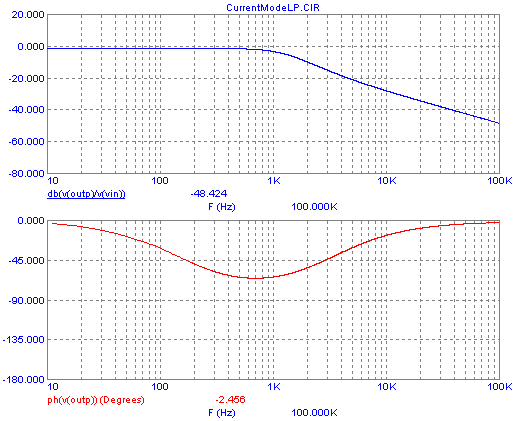
This is how the Bode plot for our LC lowpass filter, complete with ESR,
looks when the filter is driven in current-mode:
Note that the gain curve is the exact same as in voltage-mode control,
but the phase lag doesn't ever reach even close to 90°, and
returns to zero at high frequencies. The explanation for the phase
curve: At low frequency, the capacitor is an open circuit, and we are
just pumping controlled current into the load resistor. So, zero phase
shift. At around 20Hz the capacitor starts becoming significant in
parallel with the load resistor, thus causing some phase lag. But from
1kHz up, its ESR starts becoming significant, pushing the phase back up
by making resistances dominate! The inductor, which caused
a 90°
lag in the high frequency range in voltage mode, cannot do so now,
since we are controlling its current rather than a voltage applied to
it. But the inductor stays fully effective in filtering the 50kHz
switching frequency, keeping the transistor current from
spiking,
and storing energy.
Designing an error amplifier for a current-mode regulator is trivially
simple. A PI circuit with its zero placed at a somewhat lower frequency
than that of greatest phase lag works very well and is quite
uncritical. In
some cases a plain simple integrator works well enough, and that's
often seen in power supplies using simple control-mode ICs such as the
UC3842. I have also successfully used simple high gain proportional
amplifiers, which eliminates the low frequency phase lag of an
integrator, and thus avoids the problem of low frequency instability
when a battery is connected to the output, shifting the filter's
frequency way down. With a proportional amplifier, it's good practice
to add a small feedback capacitor to limit high frequency gain, to
reduce jitter. That means, place a small capacitor in parallel with the
feedback resistor, calculated to give a pole at maybe one tenth the
switching frequency. The resulting phase lag at high frequencies is
almost always well within the healthy range.
The gain of the power section in a current-mode regulator depends on
the load resistance. The higher the load resistance is, the higher is
the gain. As the load resistance goes up, also the pole formed by it
with the filter capacitor goes down in frequency. At no load, this pole
can sit in the millihertz range, causing the -90° shift region of the
low pass filter to extend into that very low frequency range. And the
gain tends to be extreme. For this reason, an integrating
error
amplifier, which adds another 90° of phase lag, can easily make the
loop unstable, and so it's undesirable in ciurcuits whose loads may
become very light. Instead a proportional error
amplifier works fine, because at no frequency the low pass filter adds
more than 90°lag, so that with the lag-free proportional amplifier we
can use essentially any gain we want, without risking instability! In
the high frequency range, our proportional error amplifier will
naturally degrade into an integrator, and cause 90° phase lag. Its pole
frequency will depend on the characteristics of the op amp used, and
the gain we have programmed: Lower gain, higher pole frequency. As long
as the pole frequency is high enough for the error amplifier's phase
lag to fall into the range where the low pass filter capacitor's ESR
has pushed the filter's phase lag back near zero, there will be no risk
of oscillation.
To avoid excessive pulse width jitter, it's a good idea to avoid
unnecessarily high error amplifier gain at the circuit's switching
frequency. Depending on the op amp we use, and the proportional gain we
program it for, we might need to deliberately reduce its pole
frequency. This is done by adding a small feedback capacitor, in
parallel with the feedback resistor. The pole frequency of course will
the one at which the chosen capacitance has a reactance equal to the
feedback resistor's value.
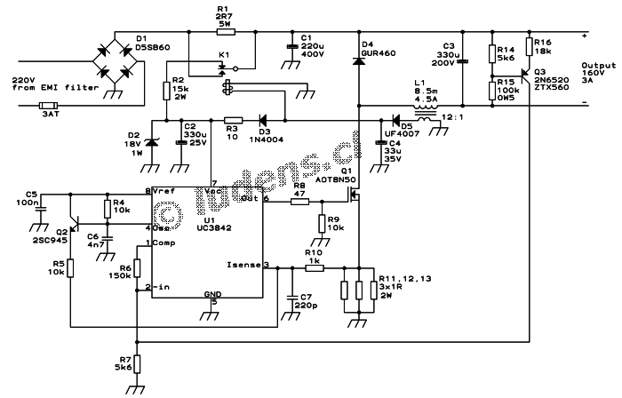
As a practical, working example of a current-mode voltage
regulator with
a simple proportional error amplifier, you might want to have a closer
look at my 160V,
3A motor power supply.
It uses the ubiquitous UC3842, and the error amplifier is a simple
proportional one, with a 150kΩ feedback resistor and a 5.6kΩ input
resistor, giving it 30dB gain. Let me use this circuit to illustrate
some of the computations in a current-mode regulator:
As you can see in the UC3842's datasheet, a 3V change at the output of
the error amplifier will make the peak current vary from zero to its
maximum possible value. This maximum value is set by a 1V internal
limit, and internal 1:3 divider, and the external sensing resistance. I
used 0.33Ω, so that
the maximum current possible is 3A. This means that the pulse width
modulator of this current-mode IC, in my configuration, will have a
transconductance of one ampere per volt, very easy to remember.
You need to be aware that the current we are controlling here is the
peak current. The average current will be lower. How much lower,
depends on the component values and the current level at which it is
operating. If the inductor is working in continuous mode, and with a
high DC current and low AC ripple current, the average current is
almost the same as the peak current. But as the current becomes lower,
due to a lighter load, the ripple current in the inductor stays
constant, while the DC current gets smaller. So, the average current
becomes smaller relative to the peak current. This becomes extreme when
the inductor operates in discontinuous mode, and the average current
can become a small fraction of the peak current. So, the real
transconductance of this contraption is nonlinear, and generally
increases with current!
Let's take the highest possible current, which produces the highest
gain. In this circuit, the average current will then be around 0.9 A/V.
Since at that level the equivalent load resistance offered by the motor
will be around 60Ω, and the current 2.7A (as you can see, I cheated a
little bit when calling it a 3A supply!), the voltage will be 160V,
caused by the 3V at the error amplifier output. This means a power
circuit gain of 35dB. Such high power circuit gains are typical for
high voltage regulators controlled by low voltage circuitry.
The feedback circuit starts with a reflex circuit that transfers a
voltage sample from the positive to the negative power rail side,
necessary due to the particular layout of this buck circuit. It has the
same attenuation as the power section has gain, that is, 35dB.
So
they compensate, and the total loop gain is just the error
amplifier's 30dB! While that may seem low, it's plenty for a
power
supply that feeds a lathe motor.
What happens at lower currents? The circuit regulates the voltage to
160V, so that's a constant (most of the time!). At lower mechanical
load the motor draws less current. At very low load, it draws only 0.2A
or so, and the inductor operates in discontinuous mode. At that level,
the average current is far below the peak current, meaning a very much
lower transconductance between the error amp's output and the inductor
current. At the same time, the higher equivalent load resistance has
gone way up, increasing the gain at that place. The two efects tend to
compensate each other to some extent, but the former is nonlinear and
the latter is linear, so the compensation can never be complete. The
good part is that thanks to the favorable phase response of this kind
of circuit, in current-mode and with a proportional error amplifer, the
loop is stable despite the highly variable loop gain.
In this circuit there is an additional complication, given by the slope
compensation introduced by Q2 and R5. It's necessary to achieve
stability in this kind of circuit, but it interferes heavily with the
power section gain calculation! If you want a good learning exercise,
take the UC3842's datasheet, assorted application notes, a circuit
simulator, and if at all possible an actual prototyping board and some
components, signal generator and scope, and work your way through it!
It will be worthwhile, I promise!
Additional phase shifts
Until here I have mostly neglected the effects of various parts of
these circuits that cause additional phase shifts. And the fact is that
almost everything causes them! In some cases they are small enough to
ignore, since the loop gain crosses zero before the total phase lag
gets to 360°, but in other circuits these additional phase shifts are
so large that they become a serious problem.
Let's start with the PWM. In addition to the delays of its internal
circuitry, given by resistances, capacitances and even tiny stray
inductances, that amount to perhaps a couple hundred nanoseconds, there
is the significant delay of PWM action itself: Changes at the
input are transfered to the output pulse length only when the next
pulse trailing edge happens. This can be from "right now" to
"one full cycle
later". So there is an average delay of one half period of the pulse
frequency, plus/minus
another half period. This means that at the circuit's switching
frequency it creates an average 180° phase lag, and at one half the
switching frequency it creates 90° lag. Given that a pole creates a lag
of 45° at the exact pole frequency, we could consider PWM time delay to
create a pole at one quarter of the switching frequency, but it's not a
nice clean pole, due to the statistical nature of this delay.
Then there is some delay in the power transistor, like a few hundred
nanoseconds, depending on its type. Let's forget that one. But a very
important additional delay in some power supplies comes from an
additional filter stage. Many switching power supplies are used in
applications where the switching-frequency ripple obtained from a
single stage low pass filter is not acceptable, and a second filter
stage is added to suppress this ripple to an acceptable level.
Depending on the component values of this a additional filter,
its
phase lag can be very bad and totally unacceptable for loop stability!
The simple solution in such a case is to take the feedback sample from
the point after the first filter, before the second one. But if high DC
voltage accuracy is desired, the voltage drop through the second
inductor might be a problem. In such a case the solution is taking the
low frequency and DC feedback from the very output of the power supply,
while taking the higher frequency feedback from before the second
filter! I did this in my 13.8V 40A power supply, with
excellent results.
Novice designers tend to love optocouplers, without even knowing them
very well. Sure, optocouplers are marvelously convenient when you need
to transfer a signal while maintaining full electrical
isolation.
But street-variety optocouplers are horribly slow! There are some
techniques to speed them up, but there is a limit. In a typical power
supply feedback loop, the delay and mid-frequency phase lag caused by
an optocoupler cannot be ignored, and their high frequency response can
be nearly nonexistent! Faster optocouplers do exist, and can be used
with far fewer problems. You just have to know it. As happens often in
life, one's first love is not necessarily the most convenient one!
Alternatives to optocouplers do exist. In some cases a transformer can
be used to transfer a signal over an electrical insulation, but when
that signal includes DC, as it usually does in a power suply, it needs
to be modulated on a carrier, and that adds complexity - and isn't
free from delay either! Another method often used in power
supplies with uncritical output stability specs is sensing the voltage
on the main transformer, and relying on reasonably good coupling for
the output voltage to follow the sensed one. This tends to work better
than many people imagine, and is extremely simple and inexpensive.
In short, it's necessary to analyze the complete circuit, with all its
obvious and non-obvious (parasitic) elements, track down and understand
all
sources of delay, and only then design the error amplifier. An
alternative to this is
Measuring the power circuit's behavior
Simulation and theoretical analysis of complicate circuits is very
prone to errors and omissions. Nothing beats measuring the actual
behavior of the real, physical circuit! A good way to do this is
opening the loop by disconnecting the output of the error
amplifier from the PWM, applying an adjustable voltage level
to
the PWM to make the circuit operate at roughly normal conditions into a
load, and injecting an small-amplitude AC test signal to the PWM. The
phases and amplitudes of the test signal at the input and output of the
power circuit are compared, to determine the gain and phase shift. This
is done at enough different frequencies throughout the spectrum, to
obtain a good idea of the power circuit's behavior. A Bode plot can be
drawn from this data. The exercise should be repeated under several
different strategically chosen operating conditions, such as full load,
no load, mid load, current limit, etc.
Specialized, multithousand-dollar test equipment is available to do
this
automatically, but it can be done easily at home, using nothing more
than a computer and a few resistors. Even a basic computer sound system
covers the spectrum to at least 20kHz, with about 80dB dynamic range,
in
stereo. That's plenty for analyzing most practical power
supplies, although some of the newer, ultracompact, relatively low
power units tend to run at such a high switching frequency that they
need analysis up into a frequency range a simple computer sound system
doesn't
cover.
Anyway, to use a computer for this task, you first get free
software
that allows generating signals, and you use it to create a test file
(WAV-PCM format is fine, don't use any lossy compression like MP3),
containing short bursts of sine waves at many different frequencies
throughout the spectrum. Start at the lowest frequency the sound system
can work at, typically a few Hz, and go up, for example, in half
octaves. Then connect your computer to the device under test, so that
the line input connects with one channel to the PWM input, and the
other channel to the power circuit's output, or if applicable you can
include the optocoupled feedback circuit in the test - just leave the
error amplifier out, and include everything else. Use the proper
resistive dividers to get signal levels compatible with a soundcard's
line input - around 1V is fine. Connect one channel of the soundcard's
line output (headphone output is OK of course) through a suitable
capacitor to the PWM input, and also connect a potentiometer there,
with its ends connected to ground and the regulated reference of your
circuit. Put the desired load on the output, and adjust the
potentiometer from zero up to get a normal output voltage. Then play
your test file, while recording the line inputs to a stereo WAV file.
Of course, use the sound system's highest sampling rate and resolution.
Then you can sit down and use any audio editing software to look at the
recorded stereo waveform, compare the amplitudes in the two
channels at each frequency, applying your voltage divider
ratios,
to calculate and plot the gain curve. And then you can time the zero
crossings of the signals in both channels - many sound editing programs
allow you to time them very accurately and easily - and you can
calculate the phase lag (or lead) at each frequency from this, and draw
the phase diagram.
And there you have your real
Bode plot for your circuit, which allows you to tailor the perfect
error amplifier for it, using the insider knowledge you gained reading
this page!
Just be sure to do the measurement at several load conditions, and
design your error amplifier for the worst case.
Error amplifier saturation and range
In addition to giving your error amplifier a suitable gain and phase
response, you also need to consider what it will do in the presence of
large signals. Sure, under normal, ideal operating conditions, all AC
signals going through the error amplifier will be small. But every
circuit sometimes goes into abnormal operating conditions. That's the
case, for example, the moment after switching it on, when the output is
totally off the correct value, because there hasn't been
enough
time yet to charge the filter capacitor. A similar situation happens
the instant something with a big capacitor in it is connected to a
power
supply: The discharged capacitor causes a severe drop of the supply's
voltage, which first has to charge that capacitor to normalize the
voltage.
There are at least two bad things that can happen in such a situation.
One is that your choice of component values isn't right for the drive
capabilities of the op amp. For example, if you use a 10Ω reference
resistor and a 100Ω resistor to get a gain of 20dB, and the op amp
works over a 5V range and has a drive capability of 1mA, you are in
trouble, because it can drive that 100Ω resistor only over a 0.1V
range! If the circuit is a PI compensator, so that you have a capacitor
in series with that resistor, it will be fine at DC and low
frequencies, but if a large high-frequency signal happens, you are
still in
trouble. While the op amp is in saturation (voltage or current
saturation), the loop is essentially open! So you need to make sure
that your feedback impedance values are high enough, so that the op amp
can drive them over the full output voltage range, even at the highest
frequencies that will be present. On the other hand, these impedance
values shouldn't be higher than necessary, because switching power
supplies are noisy places, and high impedance circuits pick up noise
much more readily. So, the best choice is to shoot for component values
that give impedances near the low limit acceptable for the given op
amp's driving capability.
The other problem is having excessive error amplifier output range.
It's a very bad idea to power the error amplifier from a ±15V supply,
while your PWM has an input range of zero to 1V! Any condition that
makes the power circuit unable to keep the output voltage just right
will make the error amp's output soar way out of the PWM's input range,
driving it to full width pulses, or zero width pulses, depending on the
case. When the power supply's output finally gets to the correct level,
the error amp will just only begin
to slew back toward the correct range, and that takes time! During that
time, the control loop is still open, the pulses are still at maximum
or zero width, and the circuit's output will far
over- or undershoot the desired voltage. So, make sure that the error
amp's output is properly limited to just the PWM's input range, or very
slightly more, by clamping its output or by limiting its supply
voltage. If you
use a well designed PWM control IC with its internal error amplifier,
the IC's designer should have taken care of this. It never hurts to
check, anyway, because several of the old, much used control ICs suffer
from this problem! And if you cook your own, you have to
design this right!
Multiple error amplifiers
Many voltage-mode PWM controller ICs, such as the LM3524 and the TL494,
have twoerror
amplifiers instead of just one. Since voltage-mode PWM systems
have no intrinsic current limiting, they need it added, or they will
blow up very easily. This is the function of the second error
amplifier. It senses the current, using a low value resistor, a current
transformer, or maybe a Hall effect sensor, and if the current
is
too
high, it takes control of the PWM away from the main error amplifier,
reducing the pulse width to keep the current from growing to a
dangerous level. The two error amplifiers are wired together through
diodes, or through open-collector outputs with a pull-up resistor.
To achieve clean current regulation at a certain maximum level, the
current error amplifier needs its own compensation network. But then it
will normally sit there saturated, since the current is smaller than
the limit, while the voltage error amp controls the PWM, and if
suddenly a short circuit happens, the current error amp first has to
slew down into range before it can take the control away from the
voltage error amp! This means that precious time is lost, during which
the current keeps growing, at the rate allowed by the filter inductor.
In such
a circuit it's necessary to carefully calculate how long the current
error amplifier will take to kick in, worst case, and make sure that
the filter inductor cannot saturate during that time (inductor
saturation would make the current grow far more rapidly!), and
that the transistors, diodes, etc, can take this overcurrent spike
without danger. The Safe Operating Area specifications of the
components need to be consulted (and understood!) for this. Some
designers are too lazy
to do it, or even to invest time in understanding this matter, and as a
result their creations tend to exhibit a rather explosive behavior.
In the mentioned ICs there is only a single compensation output for
both error amplifiers, so at least there is no way how the feedback
capacitors for an error amp could be charged to an inconvenient value.
In exchange the flexibility for creating special error amplifiers
responses is slightly limited.
By the way, the error amplifiers of the LM3524
and the TL494 are very different. The former has a main error
amplifier, which is a
transconductance amplifier with very feeble drive capability, that's
usually compensated with an RC network to ground, rather than a
feedback network. The current error amplifier instead is a very simple
device, tailored for ground-level current sensing, with a built-in
offset, that doesn't lend itself very well to
the implementation of a clean, convenient response. The TL494 instead
has two
identical error amplifiers, which behave more like real op amps, but
still have very small drive capability.
Current-mode switching regulators are intrinsically short circuit
protected, with the current limit acting within 200ns or so. For this
reason they don't need a second error amplifier, and
current-mode
control chips normally don't have it.
Dominant pole compensation
Consider the case of a multistage audio power amplifier, such as
this ultra basic bare-bones circuit. Countless millions of audio power
amps have been build that use this fundamental circuit, with various
amounts of additions and improvements:
There is a differential input stage, that works as a comparator with
high current gain. Then an amplifier stage that has both high current
and voltage gain, and then a complementary power output stage that has
just current gain. And from the output comes a feedback path to the
input differential stage, applying strong negative feedback to the
whole amplifier, thus giving it a known, frequency-stable gain, and a
low distortion. Such an amplifier is also a plain and simple servo
loop: The reference is the audio voltage applied to the input, added to
the ground level applied through a bias resistor; there is
an output that's normally applied to the speaker; there is a
voltage divider providing a sample of the output, and a
differential error
amplifier.
Such an audio amplifier could in principle be stabilized by applying
the same recipe as for our voltage regulator: Open the loop,
characterize the response, then design the error amplifier to provide a
suitable gain and phase response to the overall loop. But this isn't
very convenient in this case, because we have (and want!) a high gain
in the "power section".
An audio amplifier has another characteristic that's very different
from a switching power supply: Typically it has far larger bandwidth
than we need or want. So, while in the case of our voltage regulator we
had to do some effort to get high enough gain into a high enough
frequency range, but without making the loop unstable, in our audio
amplifier a simple PI function seems ideal, because it will
provide enough and uniform gain at audio frequencies, where we need it,
and roll off
the gain at high frequencies, where we don't want gain, to avoid RF
noise pickup and strange behavior.
But why would such an amplifier be unstable at all? There are no
inductors, and no low pass filters, right? Well.... wrong! One problem
is that the speaker is an awfully reactive load, providing a big
inductance in some frequency ranges, and a big (motional) capacitance
in others. The other problem is that everything in electronics has a
limited frequency response: Just go high enough in frequency, and stray
capacitances,
inductances, and the effects of finite propagation speed will cause a
pole
(or two, or three...), introducing phase lag and reducing the gain.
In a multistage amplifier like this, each stage has such a low-pass,
phase-lag behavior. If the stages are very different, and their poles
all fall on very different frequencies, there will be no problem,
because as we go up in the frequency spectrum, by the time the second
and third poles have added up enough phase lag to make the circuit
unstable, the first pole will have reduced the gain enough to prevent
this instability. But if we are unlucky (and electronicians usually are
unlucky in this regard!), several poles might fall on very
close
frequencies. And that's bad news! Just see this Bode plot of a simple
60dB gain amplifier where three poles fall on the same frequency, 1MHz.
Such a pole frequency would be typical for old audio amplifiers made
with rather slow transistors:
At 1MHz the gain is down 9dB down (3dB for each pole), and the
phase lag introduced by the poles is 135° (45° each). At the
critical frequency, where the total phase change is -360°, we still
have over 40dB of gain left! So, we have again managed to build an
oscillator instead of an amplifier.
The simple solution: Move one of the existing poles down in frequency -
but only
one! By how much? Easy: That single low frequency pole has to eat up
all the existing gain, plus 6 to 10dB, at the frequency where the -360°
transition occurs. Since our intentional low frequency pole will be
contributing a full 90° lag at that frequency, the other two poles
combined only need to contribute 45° each. That means, we can take
their exact pole frequency for the calculation. And you know by this
time that a single pole causes a -20dB per decade slope. Since we have
60dB gain, we need to eat up 66 to 70dB, and that would be close to
three and a half decades in the frequency range! So, let's place our
downshifted pole on 500Hz. This is the result:
As you can easily see, the gain margin is now about 10dB, and
the
phase margin is very close to 45°, so the circuit should work fine. If
you
prefer a slightly larger phase margin, just move the pole down to 400Hz
instead of 500Hz.
This is called dominant
pole compensation.
The pole we shifted down is called dominant not because it's ferocious,
cruel or tyrannic, but simply because it has the lowest
frequency of
all poles, by far, and thus dominates the behavior of the whole
amplifier!
The most practical way to implement this dominant pole compensation is
usually adding a properly calculated little capacitor between collector
and base of one specific well chosen transistor. The one we choose
would typically be the one with the highest voltage gain, and that's
the driver stage in our simple circuit. In circuits where there are
poles on significantly different frequencies, normally the lowest pole
is chosen, and lowered even more. In many cases the lowest pole is
naturally in the stage that has the highest voltage gain. And in
amplifiers having many stages, you need to place the dominant pole in
one of the first stages, because otherwise a later stage might saturate
from large high frequency signals, before the stage with the dominant
pole has a chance to shrink that high frequency signal to its due size.
Looking at the Bode plot, you might argue that now our audio amplifier
is crappy, because its
gain is flat only in the deep bass range, and then starts sloping down!
If you argue that, you are forgetting that we are talking about open
loop gain here. An audio amplifier is typically driven from about 2V
rms, and being fed by ±30V, the absolute maximum undistorted output it
might deliver is close to 20V rms. So it needs only 20dB of voltage
gain. Looking at the gain plot, you can see that the open loop gain
stays above 20dB up to 50kHz. When we now close the loop, by means of
the proper feedback resistors, to give the amplifier 20dB gain, we will
get this 20dB flat gain from the deep bass up to about 20kHz, where the
curve will start bending down. And that's optimal for an audio
amplifier! Nothing more needs to be done.
There is
an
implication, though. In the deep bass range we have 40dB
excess
gain, which will act through the negative feedback to reduce
distortion. So our amplifier will have very low distortion in that
range. But higher up in the spectrum the gain excess gets smaller, and
so the distortion will rise. In the treble range there is very little
excess gain left, and so the amplifier will have almost no distortion
correction from negative feedback there!
This is a characteristic of almost all audio power amplifiers: Rising
distortion toward higher frequencies. Now you know why this is so. The
good news is that modern transistors have extremely high frequency
response, so that it's easy and cost-effective to make amplifier stages
that
have their first poles much higher up than 1MHz. This allows placing
the dominant pole higher too, and this gives considerable excess gain
even at 20kHz, which is then shaved off by negative feedback, and thus
used to provide low distortion throughout
the audio spectrum.
Pure-blooded, slightly esoteric HiFi amplifiers typically break away
from the dominant
pole compensated, overall-feedback scheme, and use local negative
feedback in each stage. But that would be material for another web
page. This one is getting long enough as it is!
It's worth mentioning, anyway, that most op amps are stabilized by the
dominant pole method. The single compensation capacitor is internal in
most op amps, but in some it has to be added externally, and in many
others only the minimum acceptable value is provided internally, and
the relevant connections are brought out to pins, so that the designer
can add additional compensation capacitance when necessary.
Controlling other devices
Up to here I have been writing about switching power supplies,
voltage regulators and audio amplifiers, because these are the devices
I get asked about
most often. But I also told you that control loops are everywhere, and
you can apply the same techniques to many different kinds of devices.
Just a few examples:
- Temperature controllers: The defining characteristic in them is that
usually they are extremely slow, due to the long thermal time constant
of the object or room whose temperature they control. You cannot easily
make a PID controller for a home's heating system using an op amp and a
few resistors and capacitors, simply because the extremely slow
response required would call for tremendous capacitances, enormous
resistor values, along with impossibly low leakage!
One option in this case is to use a plain proportional controller,
allowing the temperature to vary within a small tolerance range. If the
sensor is placed very close to the heater, that will work, but the
temperature in the room might not be well controlled, because of the
thermal resistance between the heater and the area of the room where
you will sit (and freeze or sweat), and the thermal losses of the room.
If instead you place the sensor where you will be sitting, you get a
long delay between the heater and the sensor, which adds to the delay
shown by the heater in reacting to increased power input. The sensor
itself takes a while to react to changing air temperature. So there you
have a three pole response, causing a total -270° phase change between
ultra low frequency (hours or days) and what would be high frequency
for a thermal system (0.05Hz or so), and as a result the system would
be unstable, basically driving the heater fully on and off and making
the actual temperature go up and down a little around the set point.
Most simple room heating thermostats actually work like this.
If you want a really stable temperature, you do need a real
PID,
or at least a PI. But the very long time constant forbids the
use of analog circuits, so what you need is a PID controller
implemented in software. This allows implementing ultra slow PIDs very
easily. A tiny microcontroller costing less than one
dollar can easily manage this task.
- Industrial robots: Usually these have several axes of movement, and
each needs to position very precisely, and move as quickly as possible
between one position and the next (time is money!), but without
exceeding certain
acceleration limits. Usually this requires a double nested control loop
for each axis: There is a position sensor (could be an optical encoder)
feeding a PID controller that also might have some extra functions,
usually implemented
in software, that outputs an analog velocity signal. This signal is
taken as reference by a conventional error amplifier implemented with
analog components, that also reads a speed sensor (tacho generator)
mounted on the motor that moves this axis of the robot. This error
amplifier drives a power circuit, typically a PWM system, that powers
the motor. So we have an inner velocity loop, controlled by an outer
position loop. The position loop does the fine steering, the
acceleration limiting, etc, at a relatively slow scale, compatible with
software processing, while the inner analog velocity loop just performs
the single task of making the motor move at the exact speed commanded
at any time, regardless of load, accurately and fast. Look for
any
videos of car manufacturing plants, for example, and you will see what
I mean.
- Autopilots: In small boats, these typically use an
electronic
compass to sense where the boat is pointing, compare this to the
desired course, apply the error to a PID controller, and send
the
result to the tiller motor in the form of timed on/off pulses. In
slightly larger vessels, there is an additional position sensor on the
rudder, so we have two nested control loops: The outer one reads the
compass and decides the required rudder position, and the inner loop
reads the rudder position and controls the rudder motor to get it
right. In real ships, there is yet another, "more external" loop, using
a GPS or other navigation equipment as input device. This master loop
compares the actual course to the desired one, and decides where the
boat should point. Then the other two loops act, the middle one reading
the compass and deciding rudder position, and the innermost one
actually controlling the rudder. This allows compensating for side wind
and currents, while maintaining stability. And sailing yachts typically
also have wind vanes and anemometers providing a input to the
autopilot, which can then steer the yacht to sail at the optimal angle
relative to the wind.
Aircraft autopilots are far more complex, because they control at least
four axles: Elevator, ailerons, rudder, and throttles. They get input
from the altimeter, variometer, pitot tubes, gravity sensor, compass,
inertial navigation system, GPS, landing aids, etc. However complex
they may be, the
principles in them are the same as for the humble voltage regulating
loop: There is a system that needs to be characterized, and control
loops need to be designed that provide unconditional stability along
with sufficient
response speed and accuracy.
- Quadcopters: These are beautiful examples of control loops in action!
The inputs come from several accelerometers, an altimeter, often a GPS,
sometimes a variometer, a compass, and pilot input over the remote
control link. The outputs are just four: the speed of each of the four
propellers. The machines can do absolutely every maneuver, such as
climbing, sinking, going forward and back, left or right, and rotating,
by controlling just those four rotation speeds.
- Steam engine governors: They might be a little antique, but they are
a good example showing that control technology did not start with
electronics. Maybe you have seen old steam engines, like the "portable"
engines used on farms and sawmills around 1900, that have a
mechanical device spinning on top, consisting of two metal spheres
rotating on swing arms. The rotation is driven by the steam engine,
through belts or chains or gears, and the centrifugal force pulls the
spheres out, against a spring. This motion is transferred to a steam
valve, that controls the power of the engine. The centrifugal force and
the
spring make for a proportional control action, with inertia adding a
pole to avoid valve chatter (oscillation). Some of these governors
include a double
spring and lever mechanism, that adds a zero too. The result is
impressively stable! I have seen such steam engines run at a highly
constant speed, while driving a dramatically variable load. Only the
amount of vibration, rumble and steam exhaust changes with the load.
Do you think that this steam-and-iron control loop is antique?
It's barely 120 years old. I often watch some little
airborne devices in my garden, whose PID control loops are impressively
quick, precise, and free from self-oscillations. And they developed
millions of years ago, without using any Bode plots!!! They
can
make an electronic designer feel really lame...
Nothing more needs to be said, I suppose...
Back to homo ludens electronicus.