A portable oscilloscope
 Back in
prehistory, some time after the extinction of dinosaurs, but well
before the rise of the internet, I used to be a young, stupid student.
Despite that sorry condition, I was already very much into building
electronic stuff, and I badly needed an oscilloscope. But scopes and
young, stupid students don't find together very easily. The missing
link invariably is a certain entity universally known as money, and which
has a special predilection for evading young, stupid students.
Back in
prehistory, some time after the extinction of dinosaurs, but well
before the rise of the internet, I used to be a young, stupid student.
Despite that sorry condition, I was already very much into building
electronic stuff, and I badly needed an oscilloscope. But scopes and
young, stupid students don't find together very easily. The missing
link invariably is a certain entity universally known as money, and which
has a special predilection for evading young, stupid students.
After pondering this problem for some time, I decided to solve it as
best I could. And that was building my own scope. The feat successfully
concluded, I used it for developing my other projects, and also to fix
TVs and radios for paying customers, which eventually brought me into
the ownership of enough of the abovesaid scarce entity, to buy an old,
faulty, but repairable Tektronix dual trace scope. Helping to fix the
Tek was pretty much the last real work my little homemade scope ever
had to perform, and since then it has been living a quiet life, stored
away in one of my boxes of historical homemade equipment.
A lot of years have gone down the drain of history since those days.
I'm definitely no longer young, and fortunately I ceased being
a student too, although I'm not so sure about the third condition I
mentioned above... At any rate, I decided to give my cute
little homemade scope a second life, by publishing it on the internet
and making it world famous!
Well, I had the scope, and it still worked. But since this scope was
built in the days before CAD became available to me, the schematic
could possibly exist only on paper. Somewhere. I never throw away
anything that might eventually find some use ever again, so I
just had to have the schematic. But where? I started
searching for it in my binders of early projects. Nothing. I
have two large boxes of loose paper sheets with important stuff on
them. I checked them all. Nothing. Finally, when I searched through my
old university notebooks, page by page, I started finding portions of
the scope's schematic! As it was, I had been designing this scope
during lessons, while some professor was too boring to pay attention to
him. So, spread out on several pages in three different notebooks, I
found the complete schematic, although without full information about
all parts, and not completely "as built", but very nearly so.
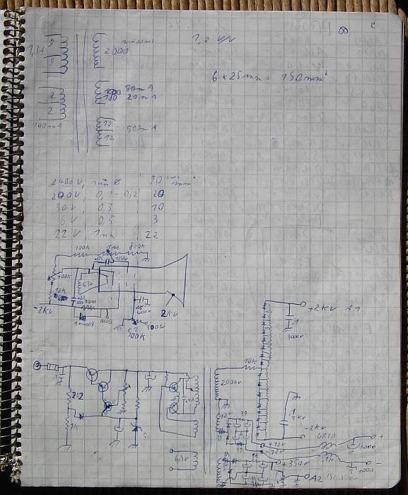
Here
you can see one of those all-important pages of scope manuscript. It
starts with a preliminary winding plan for the power transformer, then
there is the biasing circuit of the cathode ray tube, and then the
design of the complete power supply.
The CRT was biased pretty much according to the recommendation in the
tube's datasheet. I had no previous experience with CRTs, so I stuck to
the suggested circuit.
Instead the power supply is my own creation. I wanted to be able to use
this scope everywhere, including in the field where no AC power source
is available, like at mountaintops when servicing solar-powered VHF
repeaters. So I designed this scope to work from a nominal 12V. It
accepts anything from about 11V to 15 or 16V, so it can work
from a car battery or from the typical 13.8V power supply used with
radio equipment.
The scope's power supply starts with a simple linear regulator, that
puts out roughly 9 to 10V, and then it has a Royer converter that puts
out all the voltages required in the scope: A total acceleration
voltage of 4kV, equally divided into positive and negative sides; a
+350V supply to power the deflection amplifiers, and ±12V for powering
the low level circuitry. And there is also the filament winding for the
CRT, of course!
Don't worry if you can't really decipher this drawing - further down
this page is a legible version! I had enough trouble deciphering it
myself... It's a bit like reading Egyptian hieroglyphs!
And let me say at this place that I'm not
suggesting anyone to copy this scope exactly as I built it! As said
above, I was a young and stupid student, and there are a huge lot of
things that I would know better nowadays... But what I built,
sort of worked, and in those years that was good enough for me!
For example, using a linear regulator in front of a switching converter
is one of those things I would never do nowadays. Instead I would
regulate the switcher, and save several watts. Another thing is using
1N4007 diodes as fast rectifiers... They just aren't fast! So they are
somewhat lossy in this circuit. But I had to use what I could get. In
those years I didn't have a way for importing components, and
what was available in TV spare part stores in Chile back then just
didn't include many sophisticated parts.
Here is
the vertical amplifier. Actually there were three contiguous
scope-related pages in this notebook, taking the vertical amplifier
from a basic idea to a full design. The top half of this page is
irrelevant, it shows just one more idea that I did not implement.
Instead the lower half shows the amplifier, pretty much as I built it.
I still remember my big worry about how to produce the huge signals
required for the deflection plates. The CRT I got is pretty hard to
drive, requiring about 600V p-p between plates to move the spot over
the full diameter of the screen. So I needed a 350V supply for that.
But fast enough high voltage transistors able to handle that voltage
directly were simply not available to me. So I used the 2SC1921, a
200V-capable video amplifier, which was the best device I could obtain.
To handle the full 350V I needed, I put two transistors in series in
each leg of the amplifier.
So, my final vertical channel layout was: Capacitively coupled input,
switchable 1:100 attenuator, 1 megaohm potentiometer for smooth gain
control, JFET voltage follower, switchable ×10 amplifier, and then a
temperature-compensating driver amplifier and the high voltage,
differential output stage. All of it implemented with very few, and
rather cheap, components.
The experienced reader (if any) will be quick to notice that my
vertical amplifiers and attenuators lack any and all frequency
compensation. The sad fact is that such compensation was still a bit
above my head back then. I knew it was desirable, but I didn't really
know how to do it, without getting into a lot of other trouble. I would
be happy it the scope worked at all, and so I decided to work on the
"best effort" principle: In the typical way of young and brave people,
I decided to just go ahead, used VHF-capable transistors, didn't
squeeze too much gain out of each, put in no frequency compensation at
all, and hoped for the best. Do I need to tell you what the -3dB
frequency response of this amplifier turned out to be? You might guess
it. Or you might likely guess far too high. Suffice it to say that the
scope is great for displaying audio signals, and also did reasonably
well when diagnosing problems in switching power supplies and in TV
sweep circuits. Just don't ask it to get up into the RF range! That
would be like asking a pine tree to produce coconuts.
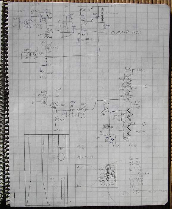
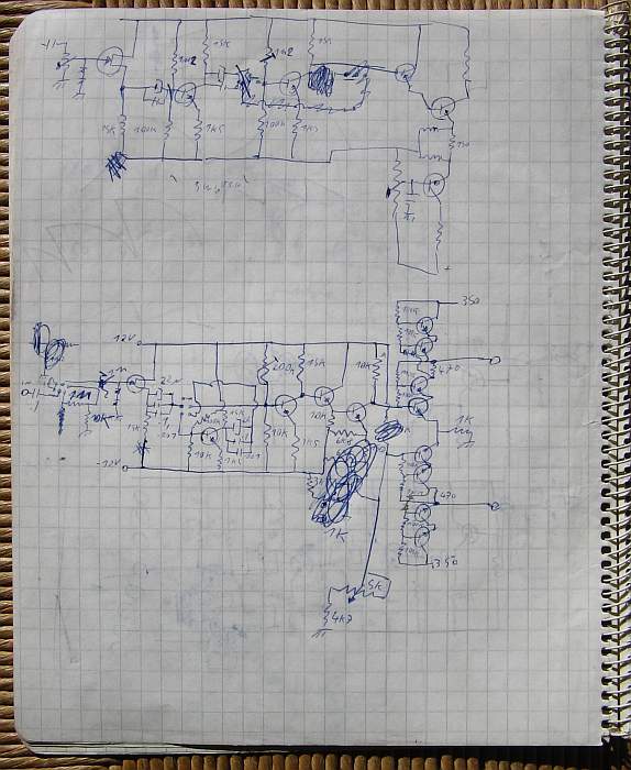
And this
is the third and last relevant page I found in my notebooks. This one
is drawn with a pencil, not a ballpen like the others. At the
top you can see one of the absolutely most clever circuits I have ever
designed with the good old 555 timer chip! Yes, it was around in
prehistory - and it was modern, back then! It performs the
task of a wide range linear sawtooth generator, with triggering, and it
even provides the retrace blanking signal for the CRT's grid!
To get a linear ramp, a PNP transistor is used as a current source, to
charge the 555's timing capacitor. There is a switch that selects
between two caps, with a 1:100 ratio between them, and the current
source is controlled by a logarithmic potentiometer, which also gives a
1:100 range. The end result is a sweep rate continuously variable over
a 1:10,000 range!
The trigger signal for the 555 comes either from one of the vertical
deflection outputs, or from the timing capacitor. In triggered mode
this results in extremely sensitive and effective triggering, giving
very good trace stability, while in free running mode it allows
fine-tuning the sweep frequency against the signal frequency, for more
convenient examination of such things as digital bit sequences.
The retrace blanking output is taken from the nominal output pin of the
555 timer, and amplifier by a high voltage transistor, in a common base
circuit, while the sweep output is taken directly from the timing
capacitor.
The middle section of this sheet shows the horizontal driver and high
voltage amplifier. The driver is simply a Darlington voltage follower,
and some adjustments for trace width and centering, while the high
voltage amplifier is a plain copy of the vertical amplifier.
The end of the page shows a preliminary drawing of the mechanical
layout of the major parts, and the front panel. My final front panel
layout ended up a bit different, but such are the liberties of the
builder!
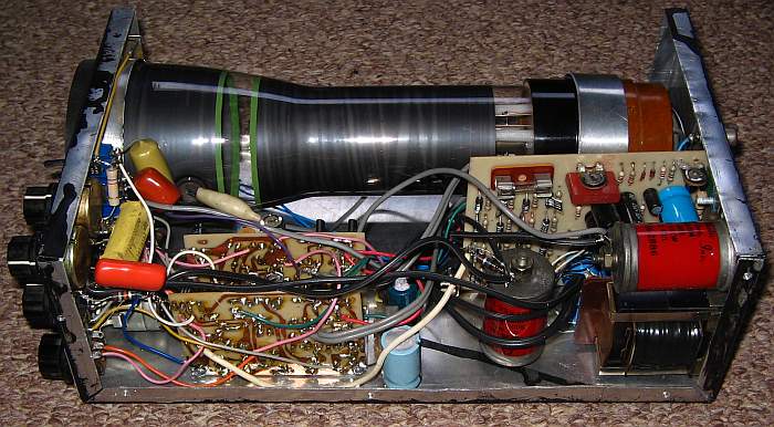
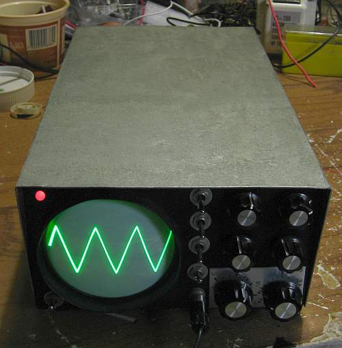
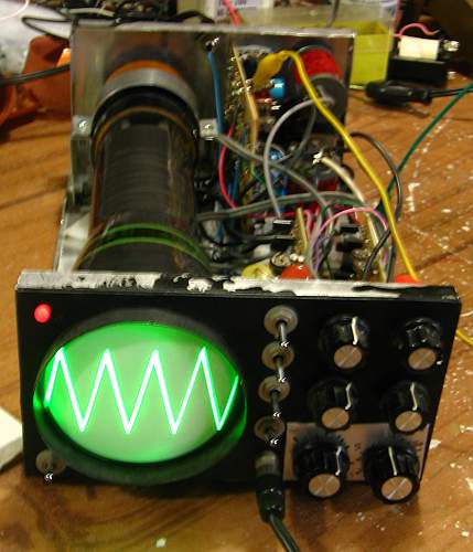
As you
can see in this picture, the length and height of the housing are
dictated by the dimensions of the CRT, while the width is given by the
front panel space required by the controls beside the screen. Instead
the circuitry is quite compact and leaves a lot of unused space in the
box.
The box is made from 1mm thick aluminium sheet. Since I was a poor
student and had to save on paint, I only painted the outside, and left
the inside in its shiny natural state.
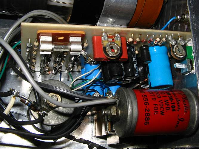
The circuitry in the rear portion is the power supply. The nice red
cylinders are 100nF, 3000V plastic film capacitors, which I got for
free somewhere. They are likely capable of a huge ripple current, which
isn't required in this circuit - but I had them, so I used
them.
In the lower right corner of this picture sits the all-important
transformer. This proved to be a problem-maker at first: It arced out
several times, because I was using recycled #42 wire for the high
voltage winding, and that wire must have been through a war or two,
because its insulation was quite scratched. All those kinks in
the wire didn't help either. Only when I finally bought some new #42
wire, which wasn't easy to find, let alone for a stupid student who
only wanted to buy a few grams of it, did the transformer work well.
Also the experience of rewinding it several times helped. There
are 4kV between the filament winding and the hot end of the
high voltage winding in this transformer, so it takes some layout
planning to get this high voltage confined to where it belongs! The
insulation material I used is plain simple vinyl insulating tape. That
was the best I could get.
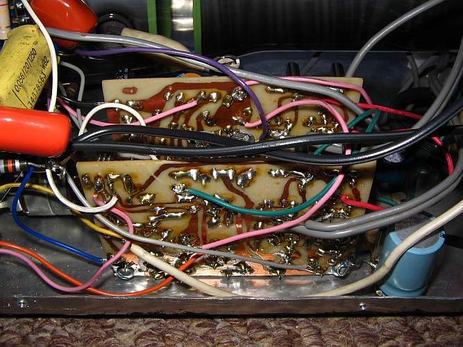
The
vertical and horizontal sections were built each on a separate printed
circuit board. Here you can see the backsides of them, and admire some
of the last PCBs I made by drawing the traces with nail polish,
directly on the bare copper! Shortly after building this scope, I
switched to the photographic process, making my positives with
transferable symbols for the pads, and narrow black self-adhesive tape
for the tracks.
An interesting detail is how I used to handle grounding issues in those
days. To keep different circuit parts from coupling through the finite
ground impedance, I made ground networks structured like trees, keeping
different amplifier stages from connecting to branches of the same
tree. All the tree trunks are rooted in one wide ground strip
at the bottom of the board, which is grounded to the chassis at least
at two places.
What you can also see quite clearly in this picture, is that I hadn't
yet developed any particularly tidy style for dressing the wires... Let
me just say that by arranging them in this airy way, both stray
capacitance and inductive coupling between them are statistically
minimized!
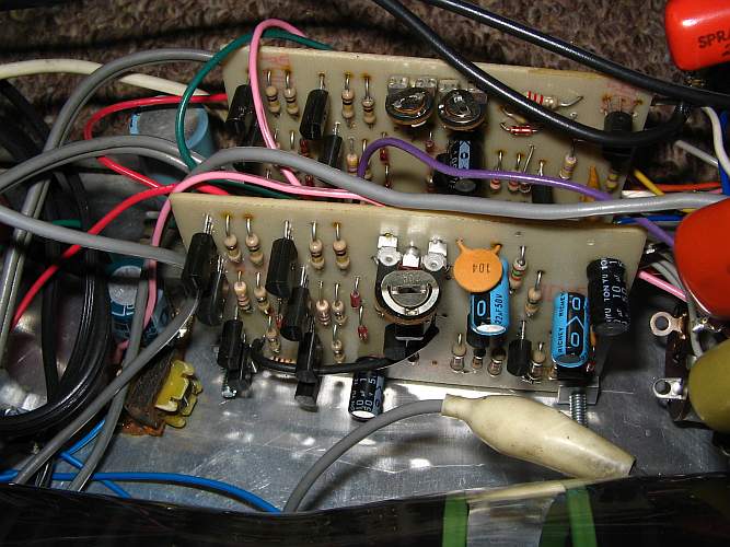
The
component side of the boards looks much better. Component layout is not
crammed, but also not particularly wasteful of space.
I used to design these PCBs with a pencil on a piece of thin
paper, overlaid on a grid in the standard 1/10" size, used in
electronics. I drew the holes as dark spots, the components as straight
lines or circles, and the traces in light gray. Then I taped that paper
to a piece of copper-clad board, drilled the holes through the paper
and the board, then I removed the paper, drew the traces free-handed on
the copper, using nail polish, then etched the boards in ferric
chloride. After washing off the nail polish with acetone, and spraying
on a layer of Kontakt SK10 solderable varnish, they were ready for
population. Quick and effective, but the paper originals were pretty
much destroyed in the process, so it didn't lend itself to series
production!
Ahhh, those were the days, before CAD!
Here is a detail of the power supply board. Tidy and compact, like the
other boards.
Did you notice that my PCB design was clever enough to place all parts
needing easy access, such as the trimmer potentiometers and the fuse,
at the top of the boards?
Instead I didn't even try to bring the input and output connections to
the edges of the boards. It was much simpler to solder the
interconnection wires directly to the relevant pads, on the solder side
of the boards.
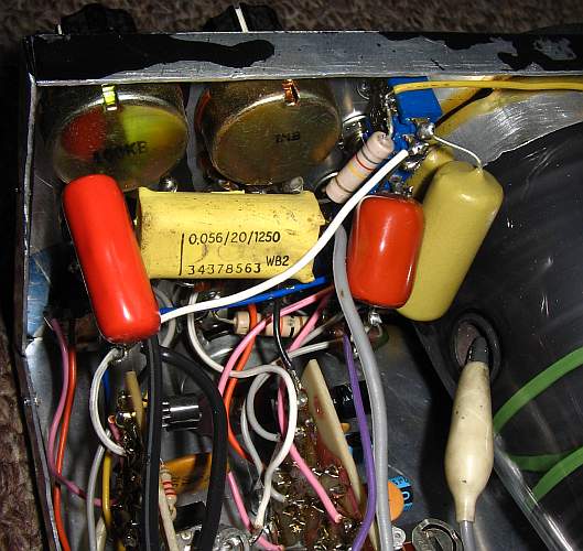
The CRT bias circuit was mostly assembled over the intensity and focus
potentiometers. There are several high voltage capacitors, which look
big and beautiful - at least to the eye of an electronician!
And here you also get a good view of my very special, highly insulated
third anode connector! It works fine, because air is a good
insulator. More worrisome is that I used just plain common
plastic-insulated hookup wire even for the high voltage lines. It seems
to work, though, and all that advice heard out there about using
special high voltage cable with thick insulation is severely
exaggerated!
The CRT I used is capable of very high brightness. It's a 3JP1, made by
DuMont. I don't know when exactly it was made, but it might be as long
ago as during WW2! I bought it in a store that sold military surplus.
It had been pulled from an old scope that was beyond repair, according
to the store owner, and he sold it complete with the socket, for
something like 3 dollars. Just what I, the young, stupid and poor
student, needed!
This CRT has a powerful electron gun, and can use over 4kV of total
acceleration voltage, which explains the high brightness achieved. When
making it work at high brightness, there is a lot of reflection of
light in the tube, so the whole screen appears green.
The tube is also pretty short, at only about 25cm! This allows my
portable scope to be as small as it is, 28×16×9cm. But a side effect of
a high acceleration voltage and short length is the low deflection
sensitivity. In fact I haven't come across any CRT needing an even
higher deflection voltage than this one! If I had gotten any choice, I
would have selected a less bright but more sensitive tube. Alas, this
was the only one I could find, and I had to be happy that I got it!
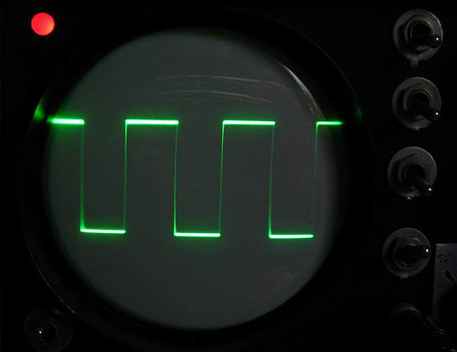
When reducing the intensity control to a more normal level,
the shine over the full screen disappears, and the little scope
displays a pretty sharp trace. There is a small amount of vertical
noise, which is 40kHz ripple from the power supply. The scope is now
several decades old, and some of its electrolytic capacitors are
probably degraded. When it was new, and if my memory isn't kidding me,
this ripple on the vertical signal wasn't there.
A funny effect is how the trace seems to extend beyond the phosphor on
the right side! That's because the ambient light was coming from the
upper right side, and there is a deep shadow on the right edge of the
screen. So there actually is
some phosphor, right to the end of the trace!
You might have noticed that the switches and most of the knobs on the
front panel have no labelling. That is a style I have been cultivating
since I started building equipment, at age 14. I find that having to
remember what each knob on each device does, is a good way to keep
one's brain in shape!
But this scope makes two exceptions to this style: The variable
attenuator, and the variable sweep frequency knobs, are fitted with
basic calibration scales. The sweep frequency scale reads directly in
milliseconds for a full sweep, while the vertical scale reads in volts
for a full display, that is, one that fills the imaginary rectange that
looks best on the round scope screen!
That way I needed no scale over the screen.
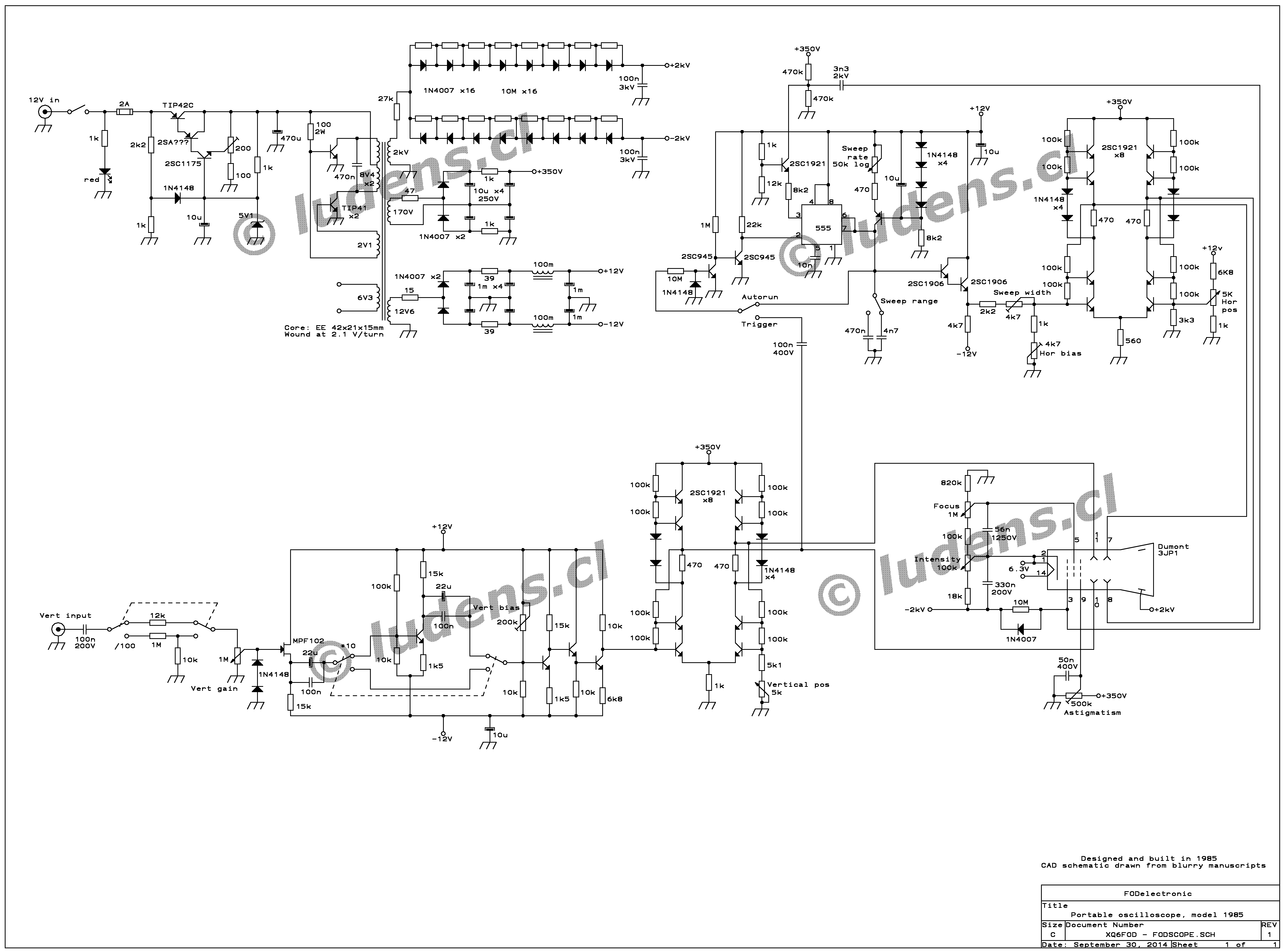
Well, you probably want to see a legible version of the schematic. Here
it is - and since the version I can display embedded in the page isn't
legible enough, you can click on the schematic to get the full
resolution version. That one is
legible, I swear!
You will notice that some of the transistors aren't identified. I
couldn't find anywhere in my notebooks what they are. Most likely I
went to the parts store, checked the lists and selected some
transistors there that were suitable, and never took the time to
back-annotate them in my schematics! And to read the print on the
transistors in the scope, I would have to remove the boards, and I was
too lazy to do that. Anyway it's probably safe to guess that
the four non-specified transistors in the vertical amplifier are
2SC1906, just like the specified ones in the horizontal voltage
follower. The two small PNP transistors, instead, one of it in the
power supply, the other in the sweep generator, must be some general
purpose ones, surely of the 2SA series, which were the cheapest
transistors I could find in that time. Common 2N3906 or similar ones
should replace them just fine.
And this, my dear reader, is how the story relating one of my long
gone youth's sins comes to its inevitable end. I hope you have enjoyed
it. Probably nobody will want to copy a design as buggy as this, but it
shows one big truth: When there is need, there is a way to find a
solution, and even young stupid students can do it!
Back to homo ludens electronicus.