For several years I have been thinking about ways to build a solid state legal-limit amplifier for amateur radio use. It's not that I would absolutely need one! I own an old National Radio NCL-2000 tube-type amplifier, that still works very well. But out of technical interest I would like to develop a solid state amplifier. This new amplifer must have at least one technical advantage over plain simple common traditional amplifiers: Either it must be ultra low cost along with respectable performance, or it might be extremely small and lightweight, extremely efficient, or anything else like that. It should be an interesting amplifier, not just a brute force tool to get high RF power. And it must meet some basic requirements: The cost shall be low enough in any case to make the project worthwhile; it must provide enough spectral quality to not be a nuisance to other hams, and it must operate either in complete silence, or with very low noise. I'm fed up with the loud whirring blower of the NCL-2000!
I'm writing this page for three purposes: To bring some order
and organization into my ideas; to allow others to
eavesdrop into my work and maybe get a good idea or two from it; and
mainly to try and start an intelligent discussion on this matter. I
warmly welcome contributions! This article contains many assumptions I
made, based on my incomplete knowledge of the
many quirks of MOSFETs, so if you find mistakes and/or
you have good ideas, please let me know! My e-mail address
is![]() .
I wrote this in november 2010, so if you
happen to read it sometime in the 22nd century, forgive me for being
out of date.
.
I wrote this in november 2010, so if you
happen to read it sometime in the 22nd century, forgive me for being
out of date.
I was considering several totally different basic ideas to build an amplifier:
- A conventional class AB push pull amplifier, whose special features lie basically in using high voltage MOSFETs and operating directly from the rectified and filtered mains voltage. If reasonably low cost MOSFETs are used, this would lead to a compact, very lightweight, low cost amplifier, having a slightly better efficiency than those using power supplies that convert the voltage. The MOSFETs could be something like the ARF1505, or perhaps some low cost switching type pressed into this service.
- Conventional class AB push pull amplifier, operating from a switching power supply that is modulated to keep the voltage just a little above the RF voltage produced. This would be relatively simple and inexpensive, and would offer reasonably small size and low weight along with somewhat better efficiency than standard class AB amplifiers. The active devices could be ARF1500, IXZ210N50L, or perhaps common low cost switching MOSFETs pressed into linear RF service.
- Water cooling: It's an advantage to be able to run a MOSFET at the highest possible power, because that reduces the number of devices, and thus the capacitances, complexity and cost. This requires the best possible cooling. Water cooling should allow running a MOSFET at higher power than with conventional heatsink-and-fan cooling. It would also essentially eliminate noise. For non-intensive use, the heat could simply be discharged into a bucket of water sitting under the operating desk! The only noise would be that from a tiny water pump.
- Class E or class F amplifier using envelope elimination and restoration: This would not be the simplest approach, but it would lead to a highly efficient, small, lightweight, silent amplifier, at reasonable cost. The MOSFETs could be RF switching types, of which Ixys has some nice ones. I actually built a scaled-down prototype, but ran into trouble. More about that comes further down this page.
- Pulse-width-modulated switching-type amplifier. This is my latest pet idea. The pulse frequency is the RF frequency, the phase information would be carried by the pulse position, and the amplitude information by the pulse width. It requires really fast switching MOSFETs and drivers, but could lead to a low cost, highly efficient amplifier. This concept can use an unregulated power supply having only mediocre filtering, without significant disadvantage.
Before starting with the main article, I would like to draw your attention toward one item first, that is often misunderstood:
This technology is very well established, to the point that many designers simply copy standard layouts and optimize the component values, instead of coming up with new ideas. This leads to copying the mistakes as well as the good ideas! One of these mistakes is the incorrect understanding and use of the typical push-pull output transformer, the kind that is wound on a two-hole ferrite core, on two ferrite tubes, or on two stacks of ferrite toroids placed side-by-side. I will explain this, and I would like to read your comments on this matter, if you have any!
This is the basic layout of the output circuit of a typical push pull class AB amplifier:
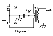
There is absolutely nothing wrong with this circuit. It works like this: When there is no drive, the transistors are biased to the brink of conduction, and the voltage on all three terminals of the transformer primary winding is Vcc. When drive starts, during one semicycle Q1 conducts a current, while Q2 is off. The current flows from the power supply through the upper half of the primary winding and through Q1 to ground. This current starts small, increases to a peak, and gets small again. At the same time, the voltage on the primary winding's upper terminal gets pulled down from the Vcc value. Due to coupling between turns, the voltage on the lower terminal, and thus on Q2's drain, goes higher than Vcc. When the amplifier is being driven just to the limit of its linear capability, the voltage on Q1's drain will reach a value very close to zero (this is the saturation voltage for that transistor), while the voltage on Q2's drain will go up from Vcc by the same amount as Q1's drain went down, reaching almost twice Vcc. The voltage on the output terminal will be proportional to that on the primary winding, with the voltage ratio given by the turns ratio. The current flowing in the secondary winding will depend on this voltage, and on the load connected. The current in Q1 will depend on this secondary current and on the turns ratio, while Q2 will conduct no current.
To put numbers to all this, let's assume the case of a 100 Watt amplifier powered by 13.8V, like those used in typical HF transceivers. Even if most of them use bipolar transistors rather than MOSFETs, the output circuit won't be different. The turns ratio in such an amplifier will be 1:4 between the entire primary and the secondary windings. When operating at 100 watts into a 50 ohm load resistance, at the waveform peak Q1's drain will be at 1.3V, and Q2's drain will be at 26.3V. This makes 25V across the primary. The 1:4 transformer raises this to 100V. On a 50 Ohm load, this makes a secondary peak current of 2A. Since the lower half of the primary winding cannot conduct any current, given that Q2 is not conducting, all of the primary current has to flow in the upper half. So we have a turns ratio of 1:8 there, meaning that the peak current flowing through Q1 will be 16A.
On the next half cycle, of course, the roles of Q1 and Q2 reverse, but the math remains the same.
Under these conditions, the 50 Ohm load sees a peak voltage of 100V, peak-to-peak voltage of 200V, and an RMS voltage of 70.71V, which produces 100W output power into that load. At the same time, the DC current consumed from the power supply is the average of the sine waveform ( not the RMS value!), which is 2/PI times the peak value. That is 10.186A in this case, so that the input power to this amplifier is 140.6W. Thus the efficiency of this stage is 71%.
If you have any experience working with radio, you will know that real world solid state broadband linear amplifiers are hardly ever as efficient as this. Efficiency is often stated as only 45%! This needs at least two explanations:
Firstly, the math I did above does not consider all losses. The only loss I considered is the one that happens due to transistor saturation being well above zero volts. But in practice there are additional losses in the transformer, feedback circuits, and also there is a small but nonzero bias current flowing, to make the stage work in class AB rather than pure class B, which wouldn't provide enough linearity. In addition, the user wants to see 100 watts at the radio's antenna terminal, so the amplifier has to deliver a few additional watts to cover losses in the low pass filter and sensing circuitry. For all these reasons, it would be reasonable to get only about 65% efficiency instead of 71%, but many practical implementations fall far short from this goal! Interestingly, many tube type linear amplifiers do have about 65% efficiency. It's not that tubes are better than transistors, nor that tuned circuits must deliver better efficiency than broadband ones. The reasons are others.
Part of this discrepancy can be explained by data sheets sometimes stating the efficiency of linear amplifier stages based on a two-tone signal, not a single tone like I assumed above. A two-tone signal gives a waveform that spends much more time at the lower voltage levels, in which a larger proportion of Vcc is dissipated in the transistors rather than being applied to the output transformer. So it's normal that the two-tone efficiency is much lower than the single-tone one. But the problem is that many practical amplifier stages used in actual radios show a lower than normal efficiency even in single-tone testing! The final stage of my 100 watt radio draws between 14 and 17A when delivering 100W, depending on the band. The complete radio draws up to 21A. That's a single-tone efficiency for the final stage between 52% and 43%! It's much too low, compared to the theoretical values for class B or AB amplifiers, and there must be a reason for this.
![]()
This photo, taken from the ARRL Handbook, shows the typical way the output transformers for such amplifiers are built. The 1-turn primary is made from pieces of metal tubing inserted in the cores, joined at one end by a piece of PCB to form a full turn. It becomes immediately apparent that this device cannot be correctly represented as shown in the schematic above! This device can be considered a single transformer only if the "center tap" (which isn't a true center tap at all!) of the primary winding isn't used! This is because it has two independent magnetic cores. The magnetic flux created by each of the metal tubes flows ONLY in the ferrite tube that covers it, and not in its neighbor. If the "center tap" isn't used, the two metal tubes are always in series, always see the same current, and so it doesn't matter whether the transformer has a single core, or two cores. But if the metal tubes can take different currents, such as happens when the "center tap" is used, then the two ferrite tubes can have totally different flux in them, effectively forming two separate transformers, with their secondaries connected in series without a tap at the connection, and the primaries connected in series with a tap!
It should be noted that the common practice of using a single ferrite core that has two holes doesn't change anything of this. Even if the ferrite is a single chunk instead of two separate chunks, the magnetic circuits around the two holes are still independent.
To make it clearer, this is the true schematic representation of a push-pull amplifier using this output transformer:
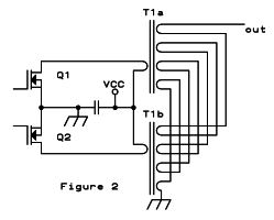
Since this drawing looks too much like a dish of noodles, we can use a simplified equivalent instead:
The important fact is that the two cores are separate, and this has serious implications on the way the circuit works.
Repeating the same analysis made for the circuit in figure 1, we get a surprise: When Q1 is starting to conduct when we just apply drive, it's pulling low the upper side of the primary winding on T1a. This makes a voltage appear on T1a's secondary, with the negative side up. This tries to make a current flow in the load, and thus also in the secondary of T1b, since they are all in series. But T1b's secondary cannot conduct a current now, because Q2 is off and so there is no place the corresponding primary current could go! An ideal transformer cannot have the current in one winding change, without the corresponding opposed change in current in its other winding. And we want T1 to be pretty close to ideal, right?
What happens then is that there flows no current in the load, and the full voltage developed on the secondary of T1a appears on the secondary of T1b, with the positive side up. So a corresponding smaller voltage appears on T1b's primary, also with the positive side up. That means, Q1 pulling its drain down from Vcc will also pull down the voltage on Q2's drain, by the same amount! The voltage on Q2's drain should go up in this situation, if the push-pull circuit were working correctly, but instead it's going down! No significant output appears across the load, but there is some net DC voltage across the transformers' primaries, which slowly starts building up a DC current in the two primaries.
So it's clear that this amplifier configuration cannot respond to fast changes in the amplitude of the RF signal! It can only respond to any form of amplitude modulation as long as the highest frequency component of the envelope is of a frequency low enough that the transformers have no significant impedance there. Instead the correctly configured circuit, with a properly coupled output transformer, is free from this problem. For SSB transmission on HF this point is irrelevant, but not in some other applications of broadband amplifiers.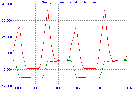 If
the transformers behave reasonably close to perfect transformers, then
T1b will inevitably win, and the current through the load will be
essentially constant during each half cycle, so that the total load
current approaches a square wave instead of a sine wave. But this still
doesn't completely explain how this amplifier can work, because
while T1b tries to force a continuous current in the secondaries while
Q2 is off, Q1 is being driven with a half sine wave, so that at first
it can conduct only a small current, then more, then more than needed,
then less again, and then too little. As a result, Q1 will saturate
over a part of the cycle, even when the amplifier is driven at a level
far lower than its maximum. And close to the zero crossings of the sine
drive signal, the drain voltages - for both transistors - will soar to
very high levels, because neither of the two transistors can conduct
the current that the transformers are forcing into that circuit, nor is
there any alternative path to ground!
If
the transformers behave reasonably close to perfect transformers, then
T1b will inevitably win, and the current through the load will be
essentially constant during each half cycle, so that the total load
current approaches a square wave instead of a sine wave. But this still
doesn't completely explain how this amplifier can work, because
while T1b tries to force a continuous current in the secondaries while
Q2 is off, Q1 is being driven with a half sine wave, so that at first
it can conduct only a small current, then more, then more than needed,
then less again, and then too little. As a result, Q1 will saturate
over a part of the cycle, even when the amplifier is driven at a level
far lower than its maximum. And close to the zero crossings of the sine
drive signal, the drain voltages - for both transistors - will soar to
very high levels, because neither of the two transistors can conduct
the current that the transformers are forcing into that circuit, nor is
there any alternative path to ground!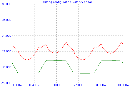 These
high voltage peaks can be brought under control by several methods. One
is applying negative feedback from the drains to the gates. This forces
both transistors to conduct a higher current when the drain voltages
rise too much around the zero crossings, having roughly the same effect
as a dynamic bias that lifts the quiescent current during those zero
crossings. In effect this moves the operating point of the amplifier
somewhat closer to class A, with its efficiency penalty.
These
high voltage peaks can be brought under control by several methods. One
is applying negative feedback from the drains to the gates. This forces
both transistors to conduct a higher current when the drain voltages
rise too much around the zero crossings, having roughly the same effect
as a dynamic bias that lifts the quiescent current during those zero
crossings. In effect this moves the operating point of the amplifier
somewhat closer to class A, with its efficiency penalty. 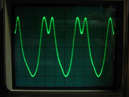 If
you don't believe my simulations, get any of the many
current transceivers that use this wrong
configuration, get a scope too, and have a look at the drain
voltage waveforms! You will see that they correspond rather well with
this simulation.
If
you don't believe my simulations, get any of the many
current transceivers that use this wrong
configuration, get a scope too, and have a look at the drain
voltage waveforms! You will see that they correspond rather well with
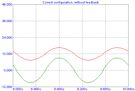
this simulation. Note that if the transistors were deliberately biased into class A, this circuit would work fine! In class A, each of the two transistors would conduct during the entire RF cycle, only in opposite phase. Each of the two transformers would see a complete sine wave with a superimposed DC component on its primary side, and a pure sine wave on the secondary side. The DC component is usually irrelevant in RF transformers, because it's no larger than the RF component, and RF flux density has to be kept very low anyway to avoid excessive loss in the core, so that the resulting low DC flux density is very far from causing saturation. So, the circuit with the two separate transformer cores works well in class A, and some designers indeed have found that they have to bias their amplifiers well into class A to get them to work, and to keep the peak drain voltage inside a safe range. The usual symptom is poor gain and dismal efficiency in class B, with normal behavior in class A. Biased into class AB, the amplifiers will have good performance up to the power level where the operation moves from class A mostly into class B, and there the gain will drop, the waveform will distort, and high drain voltage peaks will appear. This change of gain, when transitioning from class A operation into class AB, also explains the poorer IMD performance of the wrongly configured amplifiers, when compared to a correct configuration.
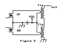
If the output transformer is built on one single core, having one single magnetic loop, such as a toroid, of course the circuit will work fine in class AB and class B too. And if the transformer is built from two separate cores, like the one in the photo, but the primary winding has two turns, with one complete turn on each side of the center tap, then it will work fine too in class AB or class B! But many circuit designers (or should I rather say "circuit copiers"?) seem to love the conventional construction style of this transformer, and copy it without hesitation nor any understanding of its behavior.Not all is lost. It's possible, and has actually been quite usual in real world radios for many years, to make a small addition to this circuit, that will solve the problem:
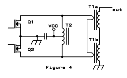
T2 is a relatively small ferrite toroid, on which a few bifiliar turns are wound. This is connected as a center-tapped choke, with its two sides being very tightly coupled, thanks to the bifiliar winding style. The amplifier is fed through this device, instead of using the incorrectly implemented "center tap" of T1. T2 is often considered to be just a DC feed choke in the literature, and many authors who have never tought about this matter consider it completely optional, but in fact in a circuit like this it's not optional at all, and its true role is quite a bit more involved!
Let's analize what happens: When Q1 conducts at the peak of its semicycle, it will have 1.3V on its drain, making 12.5V between Vcc and its drain. That places 12.5V on one half of T2. Due to the tight coupling, that forces 25V to appear across the entire T2, making Q2's drain go up to 26.3V. The primaries of T1 will see a total of 25V, that will be transformed to 100V at the output, and the 50 ohm load will take a current of 2A. Since both primaries of T1 are conducting, we have a true 1:4 turns ratio, so the primary current is 8A. These 8A come from the power supply, flow through the lower half of T2, then through the primaries of T1 and from there through Q1 to ground. Since T2 is tightly coupled, the current through its lower half is compensated for by another equal current, another 8A, flowing from the power supply through the upper half of T2, also through Q1 and to ground.
So we have the same current and voltage in the transistors and power supply as in the analysis for figure 1, and also the same power output and efficiency. The only practical effect of adding T2 is that we can now use a T1 built like the transformer in the photo, without any problems! In other words, T2 simply provides the true center tap that cannot exist on a transformer that uses two cores and only one primary turn!
In this circuit it's a good idea to place a DC blocking capacitor in series with T1's primaries. If everything were perfectly balanced, that capacitor wouldn't be necessary, but things are hardly ever really well balanced. Even a small net DC could saturate T2, since this choke is usually wound with several turns on a small core.
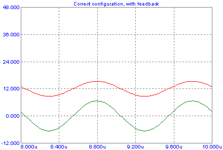
 Do
you want to see what difference this bifiliar feed choke makes?
Well, just look at this image! It's the exact same test amplifier
that produced the horrible waveforms above, with the same drive, the
same bias - but with a bifiliar feed choke added.
Do
you want to see what difference this bifiliar feed choke makes?
Well, just look at this image! It's the exact same test amplifier
that produced the horrible waveforms above, with the same drive, the
same bias - but with a bifiliar feed choke added.
 We
can of course add negative feedback to this circuit too. The result is
lower gain and better linearity, but without any fundamental effect on
the circuit's operation.
We
can of course add negative feedback to this circuit too. The result is
lower gain and better linearity, but without any fundamental effect on
the circuit's operation.
By the way, when you have more drive power available than you
need to drive your transistors, the most stupid thing you could do is
wasting that power in an attenuator! Instead it's much better to reduce
the amplifier's gain by increasing its negative feedback, because that
will make good use of the excess drive power to improve the linearity
of the amplifier! After all, in a Linear Amplifier you can never
have too much linearity...
The technical literature contains a great many examples of schematics that contain the output transformer error addressed here. Authors copy from each other, without ever actually building the circuit and testing it. So they don't notice the mistake. Or they actually build the circuits, and consider themselves satisfied with 50% efficiency in class B, failing to understand that with a correct circuit configuration they could easily get 65% or better, and improved linearity too.
And now that I have blown off enough steam on this issue, let's go on to the main part of this article!
If we want to build a high power HF amplifier, the selection of suitable transistors isn't very broad. Some jokers suggest to use the MRF154 or MRF157. At close to 1000 dollars a pair, they just can't be a popular choice. Many people prefer the MRF150 or similar ones, which are much smaller and equally old fashioned. Typically four pairs of these would be required, as a minimum. That makes for an increasingly complex amplifier.
But there are other options. Quite recently a few other manufacturers have come out with relatively high power MOSFETs rated for linear amplifier service at frequencies to 30MHz and beyond. The ARF1500 series, and the IxysRF devices, are good examples. These transistors are less expensive than the venerable and rather antique Motorola/Macom ones, but still their cost is significant. A typical ham building an amplifier will inevitably worry about burning out a set or two of transistors, before curing any infant maladies of his pet project. If the transistors cost a few bucks, that's no problem. But if each little cloud of smoke you draw costs you 2000 dollars for a quad of MRF154 transistors, it might make you think twice, at least, before embarking on the project! It doesn't make me think twice, anyway: That price is too high, period! It doesn't even deserve a second thought.
I have intensely thought about the IxysRF transistors, such as the IXZ210N50L. They have lots of things in their favor: They were designed specifically for linear amplifier use. Their power capabilities would allow making a legal-limit amplifier with reasonably few devices. Their physical shape lends itself well to simple construction with low stray reactances. And their cost, according to advertised prices, might be no more than 300 dollars for a full set that produces 1500W output. I have only two hassles with them: One is that they seem pretty unique, so that if IxysRF decides to pull them, there would be no way in the world for anyone to copy my design, nor for me to repair it, should the transistors ever fail. And the other is that these devices seem to be mostly vaporware! I haven't been able to find any distributor who would actually be able and willing to sell me a few. I wonder if these transistors are actually in production, or if they are some sort of phantom.
The ARF devices look worthwhile too, but they too are not easy to find, and they are more expensive. Also their characteristics seem to be a little less attractive than the Ixys ones, for example they have higher capacitances for a given set of conditions.
I have spent lots of time thinking about the use of plain common power switching MOSFETs for high power linear amplifier use. These are widely available, in countless different specs and shapes and colors and flavors, and they are very inexpensive. New and better ones show up all the time. Many hams have successfully used small switching MOSFETs like the IRF510 for linear RF amplification. So one might be tempted to investigate the differences between linear RF MOSFETs, and switching MOSFETs.
The differences are in fact many. Some of them are related to the "RF" factor, and others are related to the "linear" factor. Let's see:
Switching MOSFETs are optimized to have the lowest possible resistance when on, and the highest possible one when off. And they should go from off to on, and back, as quickly as possible. That's about all there is to it. Linear RF MOSFETs instead don't need to have very low ON resistance, because they will operate in their linear range, not in saturation, and a lower ON resistance would only marginally increase their efficiency. Instead they need to have the absolutely lowest possible internal capacitances, because these are always too high in MOSFETs and cause lots of trouble when operating at RF. So switching MOSFETs will have a dense gate structure, while RF MOSFETs will have a more open one.
RF MOSFETs don't need to switch quickly, and it's not even desirable for them to do so! It's better to be able to slowly and smoothly control the current. For that reason RF MOSFETs have much lower transconductance than switching ones. This is a side effect of the lower gate density too, so it goes hand-in-hand with lower capacitances.
It lies in the nature of MOSFETs that their ON resistance has a positive temperature coefficient. If two MOSFET are in parallel, and one happens to take more current than the other, it will raise its resistance and offset that effect. This has given rise to the fame that MOSFETs can be paralleled without any current sharing devices. For the same reason, the current tends to distribute evenly over the surface of a MOSFET chip. Some people forget, though, that this mechanism of current distribution works only while the MOSFET is in ON state, that is, in saturation! It does not work while the transistor is in its linear range, be it because it's in the middle of a switching process, or because it is used in linear amplifier service. Switching MOSFETs placed in parallel are usually fitted with independent series resistors at their gates, which assures adequate sharing of the switching load. But in linear service this doesn't work well enough.
While a MOSFET is in its linear range, its ON resistance (the one that has the convenient positive temperature coefficient) is irrelevant. Instead the current is controlled by the device's transconductance. And unfortunately in many MOSFETs the temperature variation of the transconductance plays against us, over most of the device's current range, and usually over ALL of the range in which it will ever be used while in linear service! In practice this not only means that switching MOSFETs running in parallel while in linear service will have severe load sharing problems, but also that a single switching MOSFET run in linear service can have load sharing problems across its surface, leading to hotspotting and destruction!
For this reason, MOSFETs designed for linear service (regardless of whether it's DC, audio or RF) need to have an internally ballasted construction. That means, there must be enough resistance built in, distributed across the device's surface, to evenly spread out the current.
Unfortunately MOSFETs for linear service have a very small market, compared to that for switching MOSFETs. As a consequence, there are few linear MOSFETs available, and they are way more expensive than their switching cousins.
Another difference is in the encapsulation. RF MOSFETs come in packages that have very low lead inductance, specially for the source leads. Normal power switching MOSFETs instead come in plain conventional packages, that have much higher inductances. Also with RF MOSFETs it's almost a rule that the device either has internal insulation from the heatsink mounting surface, or has the source connected to the mounting surface, while with switching MOSFETs that's rather an exception, with the usual configuration being the drain connected to the mounting surface. But internal insulation is very useful in RF applications, almost essential in some cases.
So, can switching type MOSFETs be used in RF linear amplifers? Or rather, does it make sense to even consider using them?
Simple answer: An MRF154 costs 450 dollars. A switching MOSFET
having the same power dissipation capability, with better voltage and
current ratings, costs 15 dollars. There ought to be a way to make it
work, don't you think?
Let's look at some basic specs for some transistors. First, I would like to compare the MRF157 linear RF MOSFET o the IXFX180N25T switching MOSFET. I chose the MRF157 simply because it's well known and available, and the other one I chose without much thinking or any selecting, looking for one that would have about the same power dissipation and have a balanced set of other features.
| MRF157 | IXFX180N25T | |
| Vmax | 125 V | 250 V |
| Imax | 60 A | 160 A |
| Pmax | 1350 W | 1390 W |
| RDSon | 75 milliohm | 12.9 milliohm |
| Transconductance | 24 S | 160 S |
| Cin | 1800 pF | 2050 pF |
| Cout | 750 pF | 158 pF |
| Creverse | 75 pF | 28 pF |
| Case | ceramic/stripline | plastic/leads |
| Insulation | No (source to tab) | No (drain to tab) |
| Cost | US$ 400 | US$ 15 |
This table makes switching transistors like this Ixys very, very appealing! Don't you think? At essentially the same power dissipation capability, it can work at twice the voltage, almost three times the current, has almost six times better ON resistance, more than six times higher transconductance (gain), only slightly higher input capacitance (which is far outweighted by the higher transconductance requiring a lower drive voltage), far lower output and reverse transfer capacitances, and it costs 27 times less money! For these big advantages one could accept the less than optimal casing, right?
But we have to look deeper than just these basic specs. First, the problem with the case. An RF transistor like the MRF157 can be bolted directly to the heatsink, and the connections are brought out to broad strips. That results in only a few nanohenries of total stray inductance. The switching transistor instead is housed in a plastic package having leads, that internally connect to the silicon chip by probably only a few bonding wires. The stray inductance could easily be 10 times higher than for the RF transistor case. If we run the transistor from an 80V supply, then the peak current will around 50A. If we happen to get 13 nH in the source lead, as suggested by some data sheets, then on the 10 meter band we get an inductive reactance of about 2.4 Ohm. So the source lead will cause a voltage drop of 120V peak! Clearly, this cannot work at all! Even just 3nH of stray inductance in the source lead would still be too much! The MRF157 instead, using its mounting surface as source connection, probably has a source inductance of less than 1 nH, so it doesn't have too bad problems in this area, as long as the circuit layout and construction is good.
Also, look that this switching transistor has the drain connected to the heat sink. Unless you use a pretty complicate circuit to place the drains at ground level, you will either need an electrically floating heat sink, which is problematic at RF, or you need to insulate the transistor from the heat sink. If you do so, the additional thermal resistance will limit this transistor to a much lower power dissipation than the MRF157 can work at.
So, the silly leaded plastic package seems to be the Achilles heel of this otherwise nice transistor!
But not only. We have to look at the other specs, and then figure out some things. First some good news: According to the data sheet, this switching transistor's transconductance decreases with temperature. That's nice, because it should make this transistor operate in linear mode without hotspotting!
But would that really work well? Its transconductance is very high. You would need less than half a volt of RF at the gate to fully drive this transistor. At such high gain, it's likely that the linearity will be pretty poor. That means heavy splatter all over the band and beyond! It might be possible to linearize the amplifier well enough by using negative feedback, but probably not as easily as it is with transistors designed for linear service. And keeping the idling current constant enough, when the transconductance is that high, is another problem on its own!
Other doubts arise regarding the propagation time along the gate structure. MOSFETs that were not designed for RF use might simply be too slow in this regard. So one end of the MOSFET chip might already be finishing conduction, while the other end is just about starting it! The transistor will be working out of step with itself if that happens. Maybe it doesn't happen, but when a transistor isn't specified for the kind of service one will put it in, one can only guess, hope, try and see!
Anyway, with the problems of the leaded plastic case, using this transistor for high power RF is a lost cause, so we don't need to even test it.
Does this mean that we cannot use switching transistors at all for RF linear amplifiers? Well, not necessarily! Two ideas come to mind, which can alleviate the problem of excessive lead inductance.
First is using the highest possible supply voltage, along with high voltage MOSFETs. This will reduce the current, and thus the voltage drop over the source lead inductance, which is essentially fixed for a given type of encapsulation. The other technique is using many small MOSFETs instead of a few large ones. Smaller cases have lower inductances, and more devices in parallel have far lower total combined inductance! Also this paralleling of many devices eases the thermal management. It's far easier to adequately cool many small devices dissipating a small amount of power each, than cooling just two somewhat bigger devices which produce as much heat as the kitchen range!
On the other hand, paralleling MOSFETs introduces problems of load sharing, and phase alignment between them. I do not particularly like to use 32 small MOSFETs in 16 separate push-pull amplifier modules, and then interconnect them using splitters, combiners, and a ratsnest of coax cables of matched lengths. It works, but it's not elegant, and too expensive. Instead I'm looking for a way to build a single push-pull stage, with many small MOSFETs on each side, that still works well enough. It could be by paralleling the drains and using separate tiny ferrite loaded transformers for the gate drive of each MOSFET, with the primaries of all of them driven in parallel or perhaps in series. The assembly would have to be compact, though, to avoid excessive phasing problems, and that runs against easy heat spreading.
Let's look at some more switching MOSFETs in TO-247 cases, rated at 1 kV, to see how the scenery looks for high voltage amplifiers with many MOSFETs. I will just choose a few available devices pretty much at random:
| APT7F100B | STW11NK100Z | IXFH12N100F | |
| Vmax | 1000 V | 1000 V | 1000 V |
| Imax | 7 A | 8.3 A | 12 A |
| Pmax | 290 W | 230 W | 300 W |
| RDSon | 2000 milliohm | 1100 milliohm | 1050 milliohm |
| Transconductance | 7.5 S | 9 S | 12 S |
| Cin | 1800 pF | 3500 pF | 2700 pF |
| Cout | 158 pF | 270 pF | 305 pF |
| Creverse | 25 pF | 60 pF | 93 pF |
| Case | plastic/leads | plastic/leads | plastic/leads |
| Insulation | No (drain to tab) | No (drain to tab) | No (drain to tab) |
| Cost | US$ 9 | US$ 6 | US$ 8 |
The idea is to run such transistors from the rectified and filtered mains, at a DC voltage of roughly 310V. In real world conditions these devices should be able to dissipate 100 to 150 watts, so that in a class AB amplifier each would run at a peak current of about 2A, average of about 0.7A. Under these conditions the source lead inductance of a TO-247 encapsulation causes only about 5V of peak voltage drop on the 10 meter band, which can be handled by the drive circuit. The ON resistance is good to, and would cause very little loss under these conditions.
But this is about where the beauty ends: Just look at the capacitances! Even taking the best of these three in this regard, we still get 25pF of reverse transfer capacitance. In a legal limit amplifier, we would need about six of these devices in parallel on each side. That makes 150pF of reverse transfer capacitance on each side. With a 600V swing on the drains, and this capacitance, Miller effect is a show killer! We are talking about six amperes of unwanted 90-degree phase shifted feedback current getting into the gates via the reverse transfer capacitance! Even if we make a drive circuit adapted to handle this, it's likely that the gate structures and connections won't like it very much. And the output capacitances are so high that we would end up with about 40 or more amperes of reactive RF current flowing in them! There is no way in the world to handle this in a broadband circuit. It would require a tuned tank circuit with a Q factor above 8 or so, much like in tube-based amplifiers.
Clearly this won't work.
Note how higher capacitance go hand in hand with lower ON resistance and higher transconductance. This is typical. For RF use we should look at MOSFETs having the lowest possible capacitances, transconductance, and thus the highest ON resistances in their class. For low frequency switching applications instead one would typically look mostly at getting the lowest ON resistance.
Let's compare to a high voltage RF MOSFET:
| ARF1505 | IXFB30N120P | |
| Vmax | 1200 V | 1200 V |
| Imax | 25 A | 30 A |
| Pmax | 1500 W | 1250 W |
| RDSon | 920 milliohm | 350 milliohm |
| Transconductance | 10 S | 22 S |
| Cin | 5400 pF | 22500 pF |
| Cout | 300 pF | 950 pF |
| Creverse | 125 pF | 28 pF |
| Case | ceramic/stripline | plastic/leads |
| Insulation | Yes | No (drain to tab) |
| Cost | US$ 270 | US$ 35 |
As you can see, the main difference is marked by lower input and output capacitances, higher ON resistance, and lower transconductance, all of these indicating a lighter gate structure in the RF transistor. The much higher reverse transfer capacitance is an anomaly. I wonder if these values simply arose from different testing methodology used for these two transistors, causing the IX transistor to show less reverse transfer capacitance in exchange for very high input capacitance.
And of course the other very important difference is the encapsulation. The switching transistor comes in a leaded plastic case with no insulation, while the RF transistor comes in an insulated ceramic case with stripline terminals. Whether the case is made of plastic or ceramic is not such a dramatic difference, but the internal insulation and the stripline terminals both make a huge difference. In practical terms, the ARF might be able to dissipate 700 or 800 watts in real world conditions, while the IX wil be limited to maybe 150 watts after adding the required insulation! And the low inductance stripline terminals allow the RF transistor to have a low voltage drop at high RF current which is far better than what the switching transistor could ever achieve.
It seems clear that for RF amplifiers we should use transistors made for that application, and not press switching transistors into that service. The problem is just that RF transistors are much more expensive, and often hard to get. When I asked a somewhat obscure distributor for a quotation, he asked how many thousand transistors I would purchase per month. When I said I needed just a few of them, one time only, he never again replied. The switching transistors instead can be ordered from many places, hassle-free, even in small quantities.
Do you like my comparison tables? Let's see one more, comparing three generations of RF power MOSFETs. One from Motorola dating to the 1970s, a much newer one from APT (now Microsemi), and the even newer one from IxysRF:
| MRF154 | ARF1500 | IXZ210N50L | |
| Vmax | 125 V |
500 V |
500 V |
| Imax | 60 A | 60 A | 10 A |
| Pmax | 1350 W | 1500 W | 470 W |
| RDSon | 75 milliohm | 187 milliohm | 1000 milliohm |
| Transconductance | 24 S | 13.5 S | 3.8 S |
| Cin | 1800 pF | 3920 pF | 622 pF |
| Cout | 750 pF | 350 pF | 77 pF |
| Creverse | 75 pF | 100 pF | 12 pF |
| Case | ceramic/stripline | ceramic/stripline | plastic/stripline |
| Insulation | No (source to tab) | Yes | Yes |
| Cost | US$ 400 | US$ 250 | US$ 35 |
The MRF needs to be powered from about 50V, while the ARF can run from anything between 50 and about 120V, having wide tolerance margins. The Ixys is much smaller - about three or four of these would make up one of the ARF or MRF, but with better capacitance ratings, lower price and better heat spreading - and higher complexity, unfortunately.
Pricewise, clearly the old MRF is too expensive to be
worth considering. The ARF is better, but still
expensive. The price stated for the Ixys is a bit of hearsay, since the
distributor stating that price is out of stock and can't supply them,
but if it is true, four of these Ixys transistors would be an
attractive alternative to one
of the others.
Why are hams still willing to use power amplifiers that have an efficiency lower than 50%? Broadcasters have long ago stopped using them! A broadcast transmitter that doesn't have at least 80% efficiency has no market chances anymore, and many exceed 90% efficiency. Energy is simply too expensive to waste it in heat while producing an RF signal! It's high time that hams would follow this trend. We should be leaders in radio technology, not late adopters, let alone naysayers!
A high efficiency amplifier would have many advantages: Smaller, lighter, possibly cheaper, lower energy consumption, longer component lifespan and reliability, lower or no fan noise, among others. And if the amplifier uses a switching scheme instead of conventional linear amplification, switching type RF MOSFETs can be used, which are more plentiful and less expensive than linear types, while at the same time all concerns about IMD and linearity move out of the amplifier block proper, and into the control circuit, which works at low power and so is far easier to manage.
I'm very fond of the idea of making a highly efficient legal limit amplifier for the HF bands. Of course it's quite a bit more difficult to make a broadband 1.8-30 MHz linear amplifier for SSB in switching technology, than it is to make a switching AM transmitter for the 0.5-1.6 MHz broadcast band, or even for the shortwave broadcast bands. Both require amplitude linearity, but in addition the SSB amp requires phase linearity, and the frequency is higher.
A relatively simple way of improving the efficiency of an amplifier is to modulate the power supply so that the amplifier gets just enough voltage for the power level it has to produce at any given instant. A good class AB amplifier is capable of producing about 65% efficiency at full power, but this decays all the way to zero, as the power level is lowered! So, a basic conventional class AB amplifier will have an overall efficiency of maybe between 20 and 45%, depending on the type of modulation, compression level, and so on. If we control the supply voltage, the amplifier could run at 100% of its possible output power (at the given supply voltage) all the time! That would allow to get a 65% overall efficiency, saving about half of the heat produced.
To do this, all that's needed is to power the amplifier from a switching power supply that can accept fast enough modulation, and one has to provide some sort of detector that produces the modulation signal.
The power supply needs to have a certain minimum voltage set, because MOSFETs sharply increase their capacitances when the voltage gets very low, and that would seriously impair linearity. But still, a class AB amplifier that has a switching power supply could be improved at very low additional cost, by adding this supply voltage modulation. The improvement in efficiency is not dramatic enough to do away with heatsinks and fans, but it's enough to warrant the small additional complexity. The savings in transistor ratings and heatsinking will probably pay for the additional circuitry, with some surplus, and the energy savings will be a freeby.
It is possible to split the driving signal into phase and amplitude components, amplify each separately, and recombine them at the output. In practice this looks like putting an amplitude detector at the input and using its output to modulate the power supply, while at the same time squaring up the drive signal and use it to drive a high efficiency, switching type amplifier, typically in class E or class F to achieve an efficiency beyond 90%. The output amplitude of this amplifier will follow the supply voltage, and the phase will be that of the driving signal. We get linear amplification with an overall efficiency (mains connector to RF out connector) of close to 80%. It almost looks too good to be true - and indeed there are serious problems in this approach!
One problem is that the RF signal path through the amplifier, and the modulation path through the switching power supply, typically have very different delay times. But at the output they need to arrive at the same time! So, some delaying of the RF signal is needed.
Worse is the problem caused by the capacitances within the MOSFETs. They are pretty large, and they change drastically when the supply voltage gets low. In low amplitude places of the waveform the power supply voltage gets very low, and the capacitances can get ten times as high as at normal voltages. Not only does this detune the output network, but also it totally wrecks the phase response! At low amplitude levels, the drive signal feedthrough gets larger than the amplified signal - and the drive signal has opposite phase! This is in addition to the phase modulation caused directly by the changing capacitances.
In 2006 I built a small scale model of such an amplifier. I believe more in practical experiment than in mathematical analysis, specially because I'm more handy with the soldering iron and the oscilloscope, than with advanced mathematics and MathCAD. The results I got were beautifully high efficiency, using common switching MOSFETs on 80 and 40 meters, but the linearity when transmitting voice in SSB was poor. The third order IMD products were down just 18dB, and that was the best I ever got. That level of splatter is ideally suited for hams who want to make instant enemies on any band they fancy to pollute.
One way to reduce this problem is to run the amplifier in EER mode only for the higher amplitude levels. For the lower amplitude parts of the signal, the power supply voltage would be clamped to a fixed value, high enough to avoid the worst phase shifting effects, and bias the amplifier into class AB. Saulo Quaggio, PY2KO, built such an amplifier and published it (QEX, July/August 2006). But he used tubes, avoiding the changing capacitances of MOSFETs! Even so, he operates his amplifier in class AB at low levels, and class F with EER only at the higher levels.
Using MOSFETs, it should be possible to run such an amplifier in pure EER high efficiency mode, by modulating both the final stage and at least the driver to it, to avoid feedthrough of drive power, and then using configurable and programmable predistortion of the phase information, most likely using digital signal processing. But this approach is far too complex to use in a simple, inexpensive, homebrew ham radio linear amplifier, and anyway it is better suited to a self-contained transmitter than to an add-on amplifier.
At this time, I don't see how to come up with a good implementation of EER for a ham radio linear amplifier, where the word "good" stands for "simple, inexpensive, with adequate performance".
So I have changed my aproach to an efficient amplifier: My concept now revolves around pulse width modulation. But not in the way audio PWM amplifiers are made, which use a high frequency carrier signal onto which the audio is pulse-width-modulated, and then a simple low pass filter at the output that passes the audio but rejects the carrier. With audio you can do that, because MOSFETS can very easily switch at the frequencies no higher than 1MHz required by this approach. With an HF amplifier instead, the MOSFETs would have to switch efficiently at least in the high VHF range, and that's a lot to ask. So my concept instead has the MOSFETs switch at the actual transmitting frequency. For this to work in SSB, it has to be done preserving the phase modulation that is present on the drive signal, and without introducing any additional phase modulation.
This is the block diagram of the amplifier I have in mind:
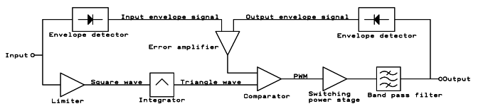
The input signal is passed through a limiter that generates essentially a square wave that has the same phase as the input (except for delays in the circuit). This in turn is passed through a simple integrator, which produces a triangle wave that has its peaks at the zero crossings of the square wave. That implies a 90 degree phase lag, but that's not a problem, because the lag is constant.
This fixed amplitude triangle wave, that follows the phase modulation of the drive signal, is compared to an error signal, obtained from the comparison of the output amplitude to the input amplitude. A PWM signal results, the pulse lengths being adjusted to get the correct amplitude at the output, while the pulse position follows only the phase changes of the drive signal. In a practical implementation, the comparator will likely have to produce two output signals, to drive the two sides of a power amplifier, but a single-ended implementation is conceivable too. The power stage is a simple but very fast switching circuit. The band pass filter reconstructs the sine wave.
The comparator cannot use much hysteresis, because that would result in nonlinearities at the low amplitude end, due to pulses dropping out entirely instead of getting narrower. Without hysteresis, it has to be a low noise comparator, to avoid as much as possible the chance of multiple pulses per semicycle. Maybe a very tiny amount of hysteresis could be used.
At very low amplitudes, it's likely that pulses will start dropping out anyway. That creates subharmonics in the output signal, and this is the reason why we need a bandpass filter rather than a simple low pass filter. With the band pass filter in place, of sufficiently high Q, and thanks to the amplitude correction loop, linearity should remain decent even down to pretty small signals. But as the signal continues to shrink, eventually there won't be enough signal for the limiter to work on, and the system will fall apart. That's no problem though, as long as it happens at an amplitude that's so low that nobody cares - let's say, 60 or 70dB below the peak power. This should be easy to achieve. The detailed design could include a circuit that completely shuts off any output pulses below a certain drive amplitude, to prevent any nonsense from appearing at the output under such conditions.
The amplitude loop needs to have a bandwidth large enough to pass all significant components of the envelope. In an SSB signal, these extend far beyond the audio bandwidth, since the envelope looks like a rectified audio signal, with sharp edges at the zero level. A bandwidth of 100kHz would be my first guess, but the scheme proposed could easily be implemented with an envelope loop bandwidth even broader than that - several hundred kHz or so. The lowest band in which the amplifier is supposed to operate is 1.8MHz, so that still gives enough frequency difference to properly separate the RF signal from envelope components.
The power supply to the power stage doesn't need to be regulated, or even very well filtered. Any hum and voltage variations will be taken care of by the amplitude loop, compensating supply voltage variations by opposing changes in pulse width. The only constraints for supply voltage would be to have enough voltage at all times to be able to produce the desired peak amplitude, and not so much that the MOSFET capacitances become too much of a problem.
All the small signal processing of this amplifier can be easily implemented. Probably it can be done even using audio-like methods, employing operational amplifiers! A wide range of pretty good RF op amps are available nowadays. The problem, though, lies in the power stage. Ideally this stage should switch very fast, compared to the RF signal period. That calls for switching times near one nanosecond, to operate well up to 30MHz! Up to a few ns might be acceptable, at the cost of reduced efficiency on the higher bands. Very fast RF switching MOSFETs are becoming available, along with suitable driver ICs, but still it's a real problem handling the MOSFET's capacitances when switching so fast. The bandpass filter following the MOSFETs must absolutely be designed in such a way that it absorbs these capacitances, and presents the proper load phase angles to the MOSFETs to achieve efficient operation. So we are talking class E or class F again, but with the added difficulty of having widely variable pulse lengths, instead of a nice steady square wave, as the source signal! I haven't analyzed this problem in depth yet, so at this moment I don't even know whether it's posible at all to solve it, or if some serious compromise would have to be reached. This point might well be the Achilles heel of this whole concept.
It should be noted that as the pulse widths get very small at low amplitudes, any MOSFETs selected will no longer be able to switch fully on and off in such a short time. This is not a problem, really. Simply the amplifier will degrade from class E or F to unsaturated class C at low signal levels, reducing the efficiency somewhat. But since it happens only at the lowest amplitudes, the losses will be nearly negligible, and the loss of amplitude linearity in the power section should be very well corrected by the amplitude loop. The only real point to watch in this area is that we need the MOSFETs and their drivers to stay symmetric in their switch-on and switch-off performance! Otherwise a phase modulation would be introduced at amplitudes low enough to prevent the MOSFETs from fully saturating, and that would seriously degrade spectral purity, because it will happen at a power level that is still significant, specially on the higher bands, where the MOSFET switching time is a more significant portion of the total signal period. This symmetry can probably be obtained to a sufficient degree by manipulating the MOSFET drivers, or at most it might require some bias applied for that purpose.
In any amplifier that separates the phase from the amplitude and recombines them at the output, like this one, it's important that the delays on the two signal paths match well enough. With supply-modulated EER amplifiers this is often a problem, because the delays of the amplitude signal through a switching power supply can be rather long. In this PWM concept, instead, the delay in the amplitude loop is much shorter. Maybe it doesn't even need to be compensated for, and if it does, that could be done using a rather modest delay line in the RF path.
Reading about such complex concepts, you might ask why not simply continue building conventional, class AB linear amplifiers, and just put up with their low efficiency. And in fact, almost all (or perhaps all!) amateur radio equipment manufacturers are doing exactly that. The ham community by and large apparently doesn't care about efficiency, power saving, and the like. There are even some retrograde hams who judge the quality of any equipment by its weight - the heavier, the better they think it is! So, why bother?
I will give you some true reasons why high efficiency amplifiers are a worthwhile goal. No, reducing your electricity bill really isn't the driving reason, as the savings will be quite small, except perhaps for really adept ragchewers. The reasons are rather like these:
- Cost: A high efficiency amplifier produces very little heat. That means using fewer MOSFETs, saving cost. Also the heatsink and fans will be much smaller, and thus less costly. The same goes for all power supply components. Unregulated power supplies can be used with some of these strategies, further reducing cost. The box will be smaller - less money spent on it. At the same time, the additional parts needed for the rather extensive signal processing as compared to a conventional amplifier, cost very little, because these are all small signal parts. In the case of the PWM amplifier, the whole pack of two envelope detectors, error amplifier, limiter, integrator, and pulse width modulator, might fit easily on less than 10cm² of printed circuit board, and cost just 10 dollars in parts. The power stage, too, is simpler than a class AB one, not requiring negative feedback, for example, nor gain compensation. The only more expensive section in the PWM amplifier, compared to a conventional one, is the bank of bandpass filters, where a conventional amplifier only requires lowpass ones.
- Size: As hinted above, such a high efficiency amplifier would be much smaller and lighter than a conventional one. That's a big bonus on DXpeditions, but also for elderly hams who can't very well lift a 35kg amplifier onto the bench!
- Stability: A switching amplifier has no issues with bias stability, because it uses no quiescent current. Conventional solid state amplifiers require lots of attention to this point.
- Parallelability: Should it be necessary to use several MOSFETs to achieve the desired power, in a switchmode amplifier they can most likely be connected in parallel, without taking any special measures. Conventional amplifiers instead typically require building several identical amplifier blocks, and join them through splitters and combiners, because otherwise it's just about impossible to get MOSFETs to properly share the load under all conditions when operating in linear mode.
And the advantages for conventinal class AB MOSFET amplifiers? They have some too, of course: Every child can take a schematic from an application note, developed by someone else and time-proven, buy the parts (as long as it's a rich child!) and assemble it. No brain effort is needed, and the results are pretty much guaranteed, as amplifiers have been built to the same designs for over 40 years. It's even possible to buy kits that have all the parts, buy the PCBs, anything. You can even buy the complete amplifiers. It's easy. But expensive, and in my opinion, rather boring.
Do you remember the Radio Amateur's Code? Part 3 of it says "The Radio Amateur is PROGRESSIVE... with knowledge abreast of science, a well-built and efficient station..."
Where does a high power class AB amplifier fit in there?
Back to homo ludens electronicus.