One typical mistake made by many amateur designers is using a transformer that has a voltage that's too low for the combination of rectifier, filter and regulator used. The situation is this: You need 13.8V at the output at all times. Your regulator eats up a certain minimum voltage, which depends on its design. Many regulators need at least 2V across them, so you need 15.8V minimum at the worst time across the filter capacitor. This is the voltage at the minimum point of the ripple waveform, but the capacitor needs to be charged to the maximum of this ripple voltage. So, the size of the capacitor defines how much additional voltage you need for this. A 60000uF capacitor, used at 20A, and discharging during almost a half cycle at 50Hz (10ms), will drop the voltage by almost 3.3V. So, you need to charge the capacitor to at least 19.2V under the worst conditions! If you are using a bridge rectifier made from silicon diodes, which loose about 1.2V each at peak current, then you end up having two diodes conducting at the time of charging the capacitor, dropping a total of 2.4V. So, the transformer needs to develop 21.6V peak voltage. This happens under heavy load, as most of the charging of the capacitor happens during a very short time, so there is a lot of voltage drop in the transformer, maybe 10 to 15%, depending on its size. So, you need to consider a transformer that develops about 24 or 25V peak voltage. Finally, you need to consider that the power line from which your design gets its power is not 100% stable! Allowing for 10% worst case sag in the power line, you end up needing a transformer that at nominal line voltage and small load provides about 27V peak! That would be 19V RMS.
If you use a transformer with a lower rating, or a smaller filter capacitor, or a regulator that has a minimum drop of more than 2V, then your power supply will loose regulation under some conditions. Many amateur designers run into this problem.
On the other hand, if you use a regulator with a lower drop, and/or a larger filter capacitor, then you can slightly ease the transformer voltage requirements. This can be very useful to keep the filter capacitor voltage rating requirement at 25V, since otherwise you would be forced to use a 35V capacitor, which is much larger and more expensive. A lower transformer voltage is also an advantage from the efficiency point of view. After all, the complete excess voltage has to be burned off by the regulator, causing a huge power loss and requiring a large heat sink!
Another issue is what kind of pass elements to use for the regulator.
MOSFETs are not a good choice, because they are much more expensive than
bipolar transistors for a given minimum voltage drop and power dissipation.
So, almost every power supply uses bipolar transistors. NPN transistors
are usually preferred over PNP ones, because they are cheaper for a given
performance, and there is wider selection. So far, so good. But most designers
place their pass transistors on the positive side, in emitter-follower
fashion, adding a Darlington driver (or two Darlington stages). This is
a very bad choice for several reasons: One, each transistor connected in
that way produces a minimum voltage drop of 0.6 to 0.7V. A three-stage
arrangement, as is often needed, would have a minimum drop of around 2V,
plus the drop caused by any equalizing resistors! Also, the transistor
collectors, which are connected to the cases, are at the unregulated positive
voltage, and thus require insulation from the heatsink and power supply
case. The necessary mica insulators add a huge amount of thermal resistance,
making it much harder to cool the transistors properly.
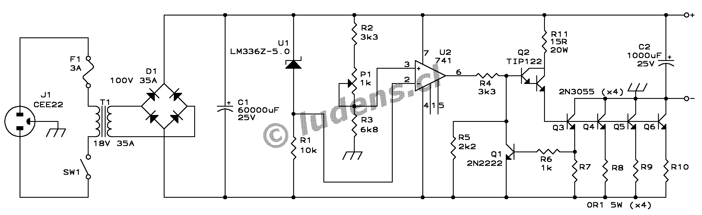
The voltage adjustment potentiometer is arranged in such a way that if the wiper contact fails, the voltage will go down, never up. This is an important safety issue, avoiding damage to connected equipment.
Here is the schematic diagram: Use the full resolution version for printing.
This power supply delivers a highly regulated 13.8V, adjustable over a moderate range, at a continuous current of up to 20A. It is current-limited to approximately 25A, and short circuit protected for as long as the heat sink can keep the transistors cool enough. It is probably the simplest design that can accomplish this.
Some notes about this circuit:
- Use a transformer for the primary voltage you need. The 3A fuse is for 220 or 240V primaries. If you use something in the neighborhood of 110V, use a 6A fuse.
- The rather high transformer rating of 35A accounts for the losses that occur due to the capacitive input filter. If your transformer is rated for capacitive input, then a 25A value is enough.
- Of course you can make up C1 by placing several smaller capacitors in parallel. Likewise, the 0.1 Ohm, 5 Watt resistors can be made up by several in parallel, for example by 5 resistors of 0.5 Ohm, 1 Watt each.
- The LM336Z-5.0 voltage reference IC should not be replaced by a zener diode. Zeners are not nearly as stable. A different voltage reference IC can of course be used, if R2 and R3 are modified for the different voltage.
- D1 and Q2 through Q6 need heatsinking. Only Q2 needs insulation. D1 dissipates up to 60W, Q2 up to 10W, while the pass transistors dissipate up to 30W each in normal use, but may reach a level of 130W during short circuit! Take this into account when choosing the heat sink!
- R5 exists only to make sure that the transistors can actually be driven off. The 741 is not a single-supply operational amplifier, so it cannot drive its output very low. If a true single-supply opamp is used, then R5 becomes unnecessary.
No parts were added to control frequency response, loop damping, etc.
All trust was placed on the 741's rather low frequency response and high
stability, combined with a 1000µF capacitor across the output. In
practice this has proven to work well enough, but purists may want to experiment
with the loop response and add some compensation capacitor.
The heat sink needs to be large. How large...? Well, it depends. Do you want your power supply to be short circuit protected without a time limit? That will require a really large heat sink!
In normal use at the 20A level there will be a bit less than 200W dissipation. The diode bridge can run at 35A when kept cool at 25 degrees Celsius (which is utopic, by the way!). As silicon can withstand 150 degrees before melting down, the 35A bridge running at 20A can survive about 75 degrees case temperature. The pass transistors are rated for 115W at 25 degrees, which means that at 30W each they can run safely at almost 120 degrees. The driver transistor can dissipate 60W at 25 degrees, so at 10W it may heat up to almost 130 degrees.
The thermal resistance from the bridge to the heat sink is probably better than 0.2 degrees per Watt, so the bridge is happy if the heat sink stays below 65 degrees. The power transistors probably have around 0.5 degrees per Watt of thermal resistance to the heat sink, so they need the heat sink to stay below 105 degrees or so. Easy. The driver transistor needs to be insulated, so with its mica insulator it will have about 1.5 degrees per Watt thermal resistance, thus requiring the heat sink to stay below 115 degrees or so. The limiting device is then the bridge. Some bridges are rated at higher temperatures, and these might significantly reduce the required heat sink size.
In the above case, you need a heat sink that doesn't warm up to more than 65 degrees Celsius while dissipating close to 200W. If you consider a highest ambient temperature of 30 degrees, then the heat sink may heat up only another 30 degrees above ambient. That is a thermal resistance of 0.15 degrees per Watt, which means a HUGE heat sink! If you really want to run this power supply at 20A continuous duty, you may be better off with a more moderate (still large) heat sink plus a small fan that blows air through it!You may use a rather small heat sink, rated for 0.7 degrees per Watt or so, if you will use this power supply for a typical HF transceiver that needs 20A peak, but at an average of no more than 5A or so. This is what many commercial power supplies do.
If you use a small heat sink, and run the power supply at high average current, you WILL burn it up. Take my word for it. Too many people have blown up their power supplies in this way.
Just for fun, lets see how much the heat sink requirement increases
if you want protection against continuous short circuit. The total power
dissipation would be around 550W. The bridge and driver transistor would
run much like they would at 25A load, while the dissipation in the pass
transistors is hugely higher than normal, reaching about 130W! As the 2N3055
is rated for 115W at 25 degrees, it means that the transistor cases would
have to be kept below 9 degrees! Considering the 0.5 degrees per Watt of
thermal resistance between each transistor and the heat sink, the heat
sink would need to stay below -56 degrees Celsius! A giant heat sink running
at the south pole maybe could just do the job, otherwise you would need
a cryogenic system! Needless to say, it is impractical to implement indefinite
short circuit protection in this way. It would become practical if you
increased the number of pass transistors, increasing proportionally the
equalizing resistors' values, but even then it would require a large heat
sink. A foldback current limit would overcome this problem, but it brings
along other problems of its own, like the power supply shutting down when
charging a capacitor in some equipment. I believe that the best compromise
is to build this circuit as shown, using a reasonably oversized heatsink,
and shut it off quickly when a short circuit happens, before the transistors
can overheat. After all, a 25A short produces a spark that's obvious enough
to notice!
The quality of the voltage regulation depends mainly on how you build this project. The single most important factors for good regulation are that the ground connection of R3 must go DIRECTLY to the negative output connector, while the top of R2 and of U1 must go directly to the positive output. Everything else is less important.
I suggest that the case is connected to the negative output ONLY via the pass transistors' cases, in order to avoid any ground loops.
This is a nice beginner's project, as all components are easily available all over the world, the cost isn't extreme, the circuit is very simple, and the resulting power supply will be useful for an entire ham radio career. For more advanced builders, I suggest to try the 40A switching power supply, which is much more elegant, efficient, powerful, smaller and lighter, costs about the same to build, but is much more complex.