80 Watt FM stereo broadcast transmitter
Before we start:
I'm well aware of the pirate radio scene that
exists in a number of countries. While I'm one hundred percent in favor
of free speech, I'm also one hundred percent convinced that the radio spectrum
has to be organized and controlled, in order to avoid interference and
allow fair access to all interested. For this reason, I ask my readers
to abstain from using my work to set up any sort of clandestine, pirate,
non-licensed radio station. On the other hand, anyone playing fair, and
doing things according to the law, is welcome to use my design.
History of this project
In Chile a significant proportion of broadcast stations use handmade transmitters.
The quality varies. Some transmitters are well made, others are very poor,
and there are also some which are well designed but poorly built, which
is the typical result of a bad technician having tried to copy a design
made by someone else.
In 2002 I was asked to repair a transmitter which was a particularly
poor example of the genre. The owner told me that this very bad thing was
the best he could afford. I told him that a much better transmitter could
be built for less money. One thing lead to the next, and I committed to
develop a high quality, inexpensive transmitter for small FM stations.
During the next months I designed, built and debugged the three main
modules of my transmitter: The audio processor and stereo encoder board,
the synthesized exciter, and the power amplifier. But when I was at that
point, my dear friend with the lousy transmitter went out of business,
and so there was no real use anymore for the transmitter I was building!
This led to the project being shelved, despite the fact that only the rather
simple control circuit was still missing.
The three completed modules have been lying around in my workshop for
four years. In my city the dial is filled up with stations which transmit
mostly very low quality music, and everyone seems to agree that there is
just no room, neither spectrum-wise nor in number of listeners, for an
additional station that would transmit good music... And anyway, I don't
have the time to run a broadcast station, not even a semi-automated one!
So there is no real motivation for me now to complete the transmitter project.
Instead of throwing everything away and forgetting it (which is something
I cannot do anyway!), I have now decided to put the design in the public
domain, so at least someone out there might benefit from the time I invested.
The concept:
This transmitter was designed from the ground up to provide very high sound
quality, coupled with excellent frequency stability, reliability, etc.
It can be used as a standalone transmitter to serve a medium-sized town,
or as an exciter to drive a kilowatt-class power amplifier to serve a large
city. It is designed to work from 13.8V nominal voltage, so that it can
be run from a common communications power supply in parallel with a backup
battery. In the event of a power cut, the transmitter can keep operating
from the battery, at slightly reduced power as the voltage drops.
It consists of four modules, the three most important of which are ready,
tested, and described below. The fourth module has not yet been built,
and might never be built, but I will describe its basic functions so that
you can design it, if you want.
So, let's start!
The audio processor and stereo encoder
The RC4200 analog multiplier used in this stereo encoder
seems to have gone out of production. Before considering the construction
of this circuit, make sure you can actually find this IC, or else be sure you
know how to modify the circuit to use a different analog multiplier, such
as the AD633 or other one you might find.
The textbook way of processing and encoding a stereo signal for FM transmission
goes like this:
1) Take both channels and low-pass-filter them at 15kHz, with steep
rolloff;
2) Apply pre-emphasis. Depending on the part of the world, it should
have either a 75µs or a 50µs time constant;
3) Strictly limit the audio level to ensure that overdeviation cannot
happen;
4) Create a stable, clean 38kHz sine wave;
5) Subtract the right channel from the left channel, and multiply the
result with the 38kHz carrier;
6) Create a clean 19kHz sine wave, phase-locked to the 38kHz one;
7) Add the left channel, right channel, the (L-R)*38kHz signal, and
the 19kHz signal, with specific amplitudes.
There are several ways to implement this algorithm. Modern factory made
transmitters often do the whole thing digitally, in a DSP. But it's still
less expensive and simpler to do in the analog domain. That can be done
in various ways too, and far too many transmitters these days use ultra
cheap, mediocre methods like hard-switched multipliers based on CMOS switches.
They do work, but are very noisy! My design instead uses a true, high quality
analog multiplier for that task. As a result, the signal from my transmitter
is as good as the very best signals I can receive locally, and MUCH better
than the bulk of them!
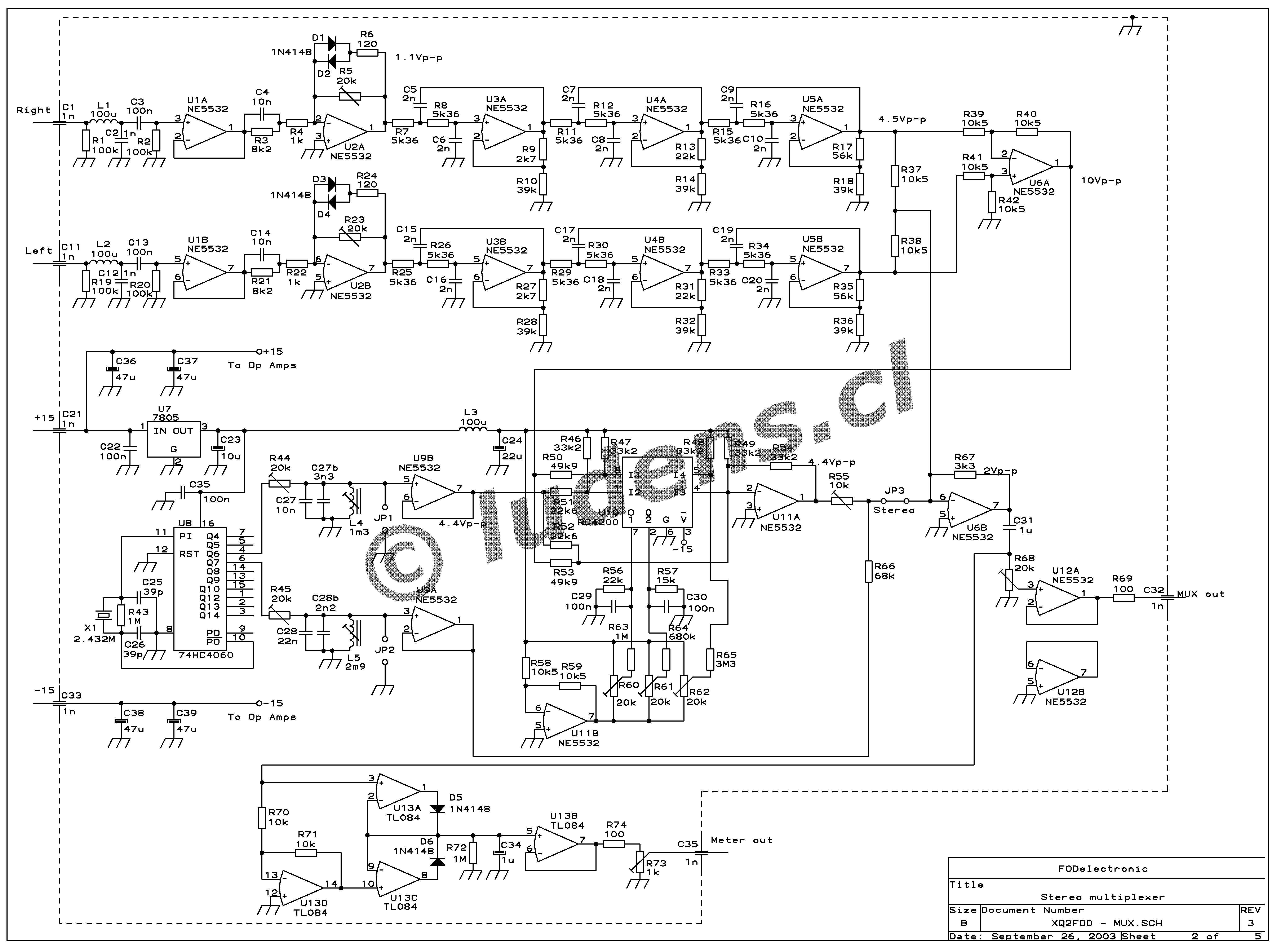
Here is the schematic diagram. You probably won't be able to read it
at this resolution, so better click on it, save it in full resolution,
print it, and refer to it for the following explanation. If you have
trouble opening the large version, right-click on the diagram, so you can
save it to disk, then open it using IrfanView or any other GOOD image viewer.
This is valid for all drawings on this page. The full resolution drawings
are large, and depending on the amount of memory in your computer, some
web browsers cannot open them and will report a broken link.
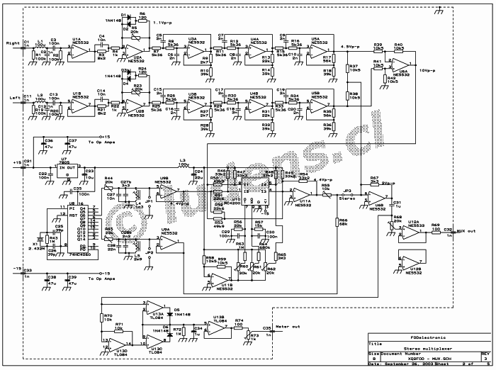 The
two single-ended line-level audio signals enter through feedthrough capacitors,
and are welcomed by an LC low-pass filter to get rid of any RF that could
be on them. In each channel there is a buffer stage, and then a combined
pre-emphasis and soft limiter stage. The advantage of doing the limiting
and the pre-emphasis in one step is that it avoids overdeviating from loud
treble sounds, or having loud bass sounds flatten out the treble, without
the need of a multiband limiter. The gain of the non-limited portion of
the audio signals is adjustable by means of trimpots. Then comes a six-pole
low pass filter that removes signals above 15kHz.
The
two single-ended line-level audio signals enter through feedthrough capacitors,
and are welcomed by an LC low-pass filter to get rid of any RF that could
be on them. In each channel there is a buffer stage, and then a combined
pre-emphasis and soft limiter stage. The advantage of doing the limiting
and the pre-emphasis in one step is that it avoids overdeviating from loud
treble sounds, or having loud bass sounds flatten out the treble, without
the need of a multiband limiter. The gain of the non-limited portion of
the audio signals is adjustable by means of trimpots. Then comes a six-pole
low pass filter that removes signals above 15kHz.
A 74HC4060 chip derives the 38kHz and 19kHz signals, as square waves,
from a custom-made quartz crystal. Two resonant circuits using ferrite
pot cores turn these square waves into very clean, low noise sine waves.
Trimpots allow to set the levels, while the adjustable cores of the inductors
allow precise tuning. Jumpers allow to disable each of these signals for
testing and adjustment purposes.
A rather old fashioned, but low-noise and low-distortion analog multiplier
chip modulates the L-R signal, produced by an op amp differential amplifier,
onto the 38kHz subcarrier. This circuit has three adjustments for balance.
Its output level is adjustable too. The signals that are necessary only
for stereo can be disconnected for testing by means of a jumper.
The output adder combines the L signal, R signal, (L-R)*38kHz signal,
and the pilot tone. The first two signals are fixed at this stage, while
the (L-R)*38kHz can be adjusted by its own trimpot, and the pilot tone
by the trimpot before its LC circuit. Then there is a final level adjustment,
used to set the deviation of the transmitter, and then a buffer stage with
low output impedance, that drives the output through a resistor to avoid
instability from capacitive loads.
There is an additional circuit which consists basically of a dual superdiode
detector with a time constant and driver with adjustable output. This circuit
picks up the complete multiplex signal just before the final level control,
and produces a DC signal to directly drive a small meter, for deviation
indication. This is a most important tool for the transmitter operator
to set the proper audio level during routine operation!
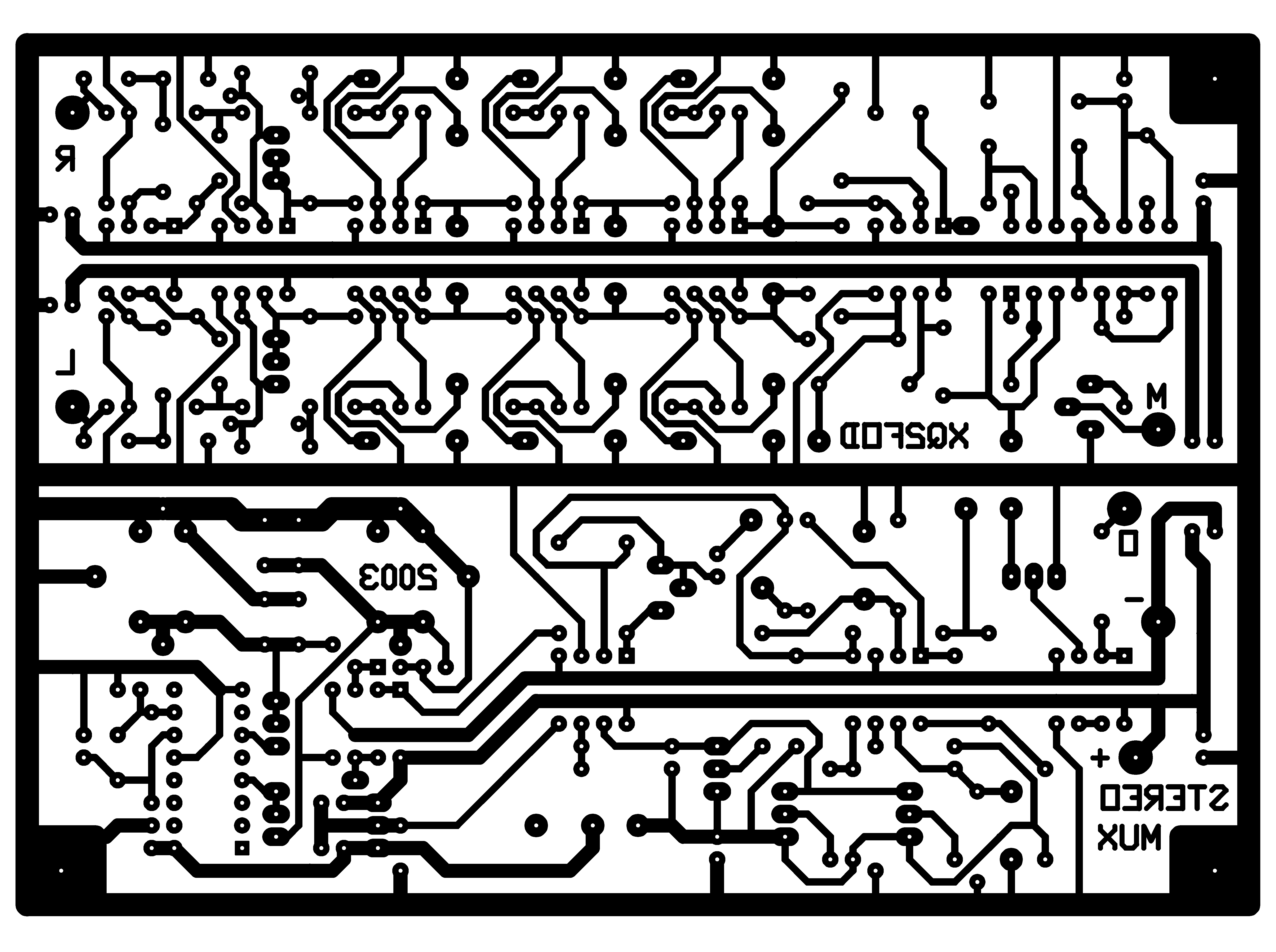
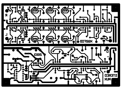 Here
is the printed circuit board. Click on it to get it in high resolution....
It's seen "through the board", so you can print it directly and place the
ink in contact with the copper to get a correct sided copper pattern.
Here
is the printed circuit board. Click on it to get it in high resolution....
It's seen "through the board", so you can print it directly and place the
ink in contact with the copper to get a correct sided copper pattern.
The entire circuit is built on this single-sided PCB. Only a few jumper
wires are necessary, so it's not worthwhile making a dual sided PCB for
this.
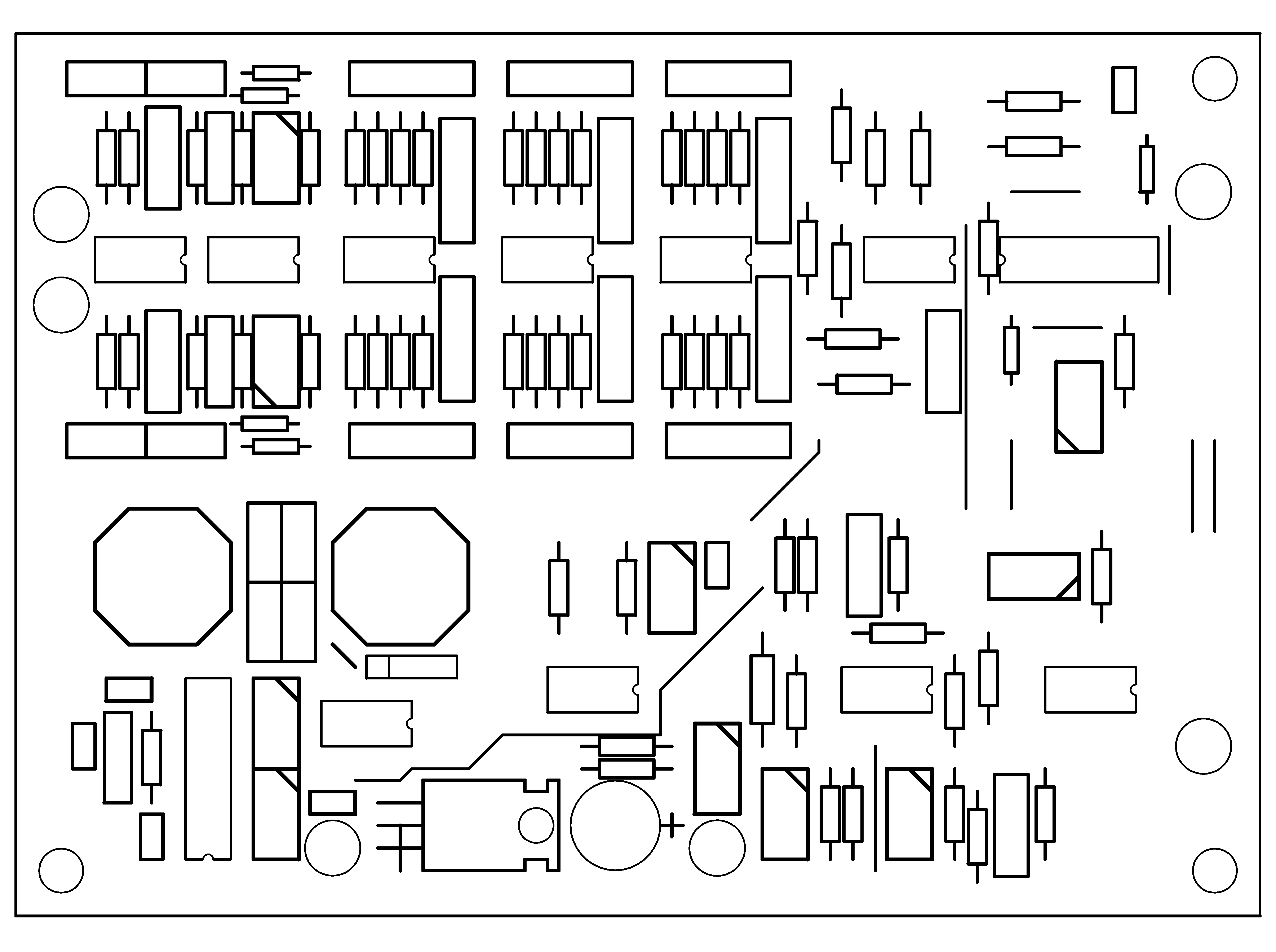
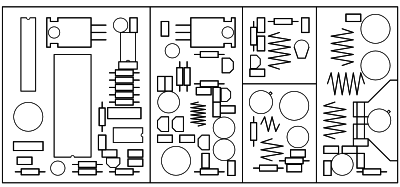
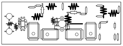
 And
this is a crude parts overlay, just to see where a part goes. Exactly which
part goes where, is something you will have to work out with the schematic!
Don't be lazy!
And
this is a crude parts overlay, just to see where a part goes. Exactly which
part goes where, is something you will have to work out with the schematic!
Don't be lazy!
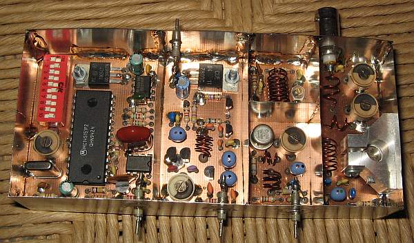
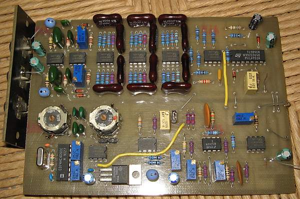 And this is how
the complete stereo encoder looks. Here I had temporarily soldered an old-fashioned
phono connector board to the inputs. Later on, the PCB should be encased
in a shielded box, with all inputs and outputs going via feedthrough capacitors.
And this is how
the complete stereo encoder looks. Here I had temporarily soldered an old-fashioned
phono connector board to the inputs. Later on, the PCB should be encased
in a shielded box, with all inputs and outputs going via feedthrough capacitors.
About the components: All of the critical resistors are metal film,
1% tolerance, both for stability and for low noise. The operational amplifiers
are a low distortion, low noise type, except for the opamp of the metering
circuit, which is a simple BiFET type. All trimpots are high quality multiturn
units. The capacitors are mostly polyester, but in the low pass filter
I used 5% silver mica ones, simply because I had a big lot of them and
could match the values very well! Matching the capacitors is a good idea,
because their 5% tolerance is a bit wide for obtaining the optimally flat
filter response. In uncritical places you will find ceramic and electrolytic
capacitors. The chokes are dipped ones removed from a junked VCR, but similar
ones can be bought new. The ferrite pot cores came from the stereo decoder
of an old (wooden boxed!) radio, which I got in a condition too incomplete
to restore. I don't have information on them, so you will have to select
your own cores and calculate the number of turns to obtain the inductance
stated on the schematic. Just be advised that the pot cores MUST have a
significant air gap, in order to be stable enough. The crystal can be ordered
from JAN Crystals, specifying a frequency of 2.432 MHz, fundamental
mode, parallel resonant, 30pF load capacitance, HC-49 holder, with standard
temperature, stability and tolerance ratings.
You have to understand this circuit to be able to calibrate it properly.
And you need an oscilloscope, of course! The process starts by presetting
all adjustments to their mid points, applying a +/-15V power supply, and
an audio sine wave of 1kHz to both channels, at a level of 1V peak-to-peak.
Set R5 and R23 for exactly 4.5V p-p at the outputs of the low pass filters,
as noted in the diagram. Then you adjust L4 and R44 repetitively while
looking at the output of U9A, tuning the coil for maximum signal and the
trimpot for exactly 4.4V p-p. Then you apply the 1kHz signal to only one
input of the board, and you short the other input to ground. With the oscilloscope
at the output of U11A, you should see a classic two-tone signal. Now you
adjust R60, R61 and R62 repetitively for best ground centering, symmetry
and linearity. This is easiest to do by using a dual channel scope and
putting the other channel on the input signal to the analog multiplier
(output of U6A), superimposing the two traces. After adjusting the gain
of the scope channels, the modulated two-tone signal should precisely fill
the 1kHz sine wave.
Now install a jumper on JP2 and put the scope on U6B's output. There
you will see the sum of the 1kHz signal and the dual-tone signal coming
from the multiplier. Adjust the level of the (L-R)*38kHz signal with R55,
so that it is exactly equal to the 1kHz signal's level. That's very
easy, because when the setting is right, the 38kHz signal always moves
between zero volt and the instant level of the 1kHz sine wave. So, you
only have to adjust the trimpot to get this zero volt line nice and straight!
If you have never built a circuit like this, you may not understand now
what I mean, but it will become clear immediately when you are playing
with the adjustment! Be sure to make this adjustment with best precision,
because the good stereo separation of this encoder depends on it!
Now remove the jumper on
JP2 and install it on JP1. Apply the 1kHz 1V signal to both channels. Tune L5
for maximum 19kHz signal, and set R45 so that the pilot signal on the scope is
about 10% the amplitude of the 1kHz signal. Now place the two scope probes on
the outputs of U9A and U9B, remove the jumper from JP1, and retouch L5 to align
the phases of the two sine waves, so that the zero crossing happens at exactly
the same time. Increasing the scope gain on the 19kHz signal helps in getting
the waveforms more parallel to obtain better precision.
R68 will be adjusted once the exciter is complete. For now, just set
it to about mid range, which will give about 1V at the output. If you already
have your meter for the deviation metering (any panel meter from 10uA to
1mA full scale should work), you can draw a scale for it and adjust R73
so that it reads 100% deviation (or 75kHz, whatever you prefer). Do this
with a signal of more than 1V applied to the inputs, so that the signal
is being limited. By the way, the reading should be the same regardless
of whether you apply the audio signal to only one inputs, or to both. When
there is no audio input, the meter should read about 10% of the full deviation
value. This is the pilot tone, and you might want to mark its level on
the meter.
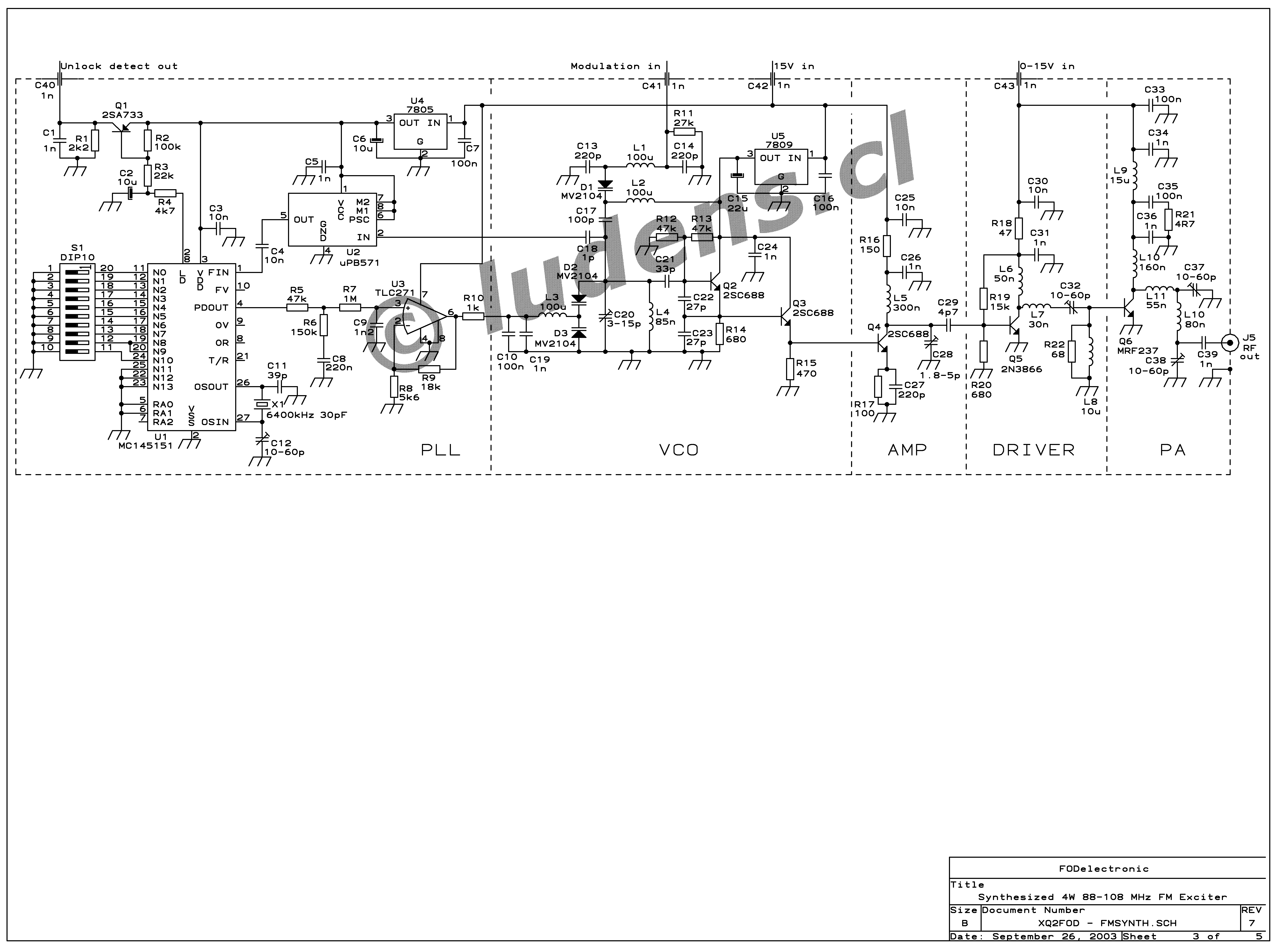
The synthesized exciter
Errata: The transistors identified as
2SC688 in the schematic are really 2SC668! Thanks for reporting the
inconsistency, Fausto!
The exciter has the functions of providing a stable, low noise, frequency-selectable
RF signal, modulate it with the multiplex signal provided by the audio
board, and amplify it to a controllable output power sufficient to drive
the power amplifier. My exciter uses a PLL frequency synthesizer, which
covers the FM band in 100kHz steps. The VCO covers only a few MHz without
readjustment, resulting in low noise. Modulation is performed independently
of frequency control, and with special consideration for low noise. The
output power is controllable from zero to 4 watts. A PLL unlock detector
is included, to shut down the transmitter in the event of a malfunction.
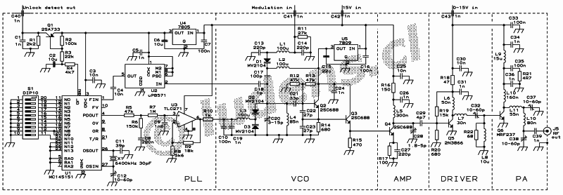 The
hearth of the exciter is a Colpitts VCO. It is powered from a local 9V
regulator, and has the frequency controlled by two back-to-back varactors,
resulting in minimal loading and thus ultra low phase noise. A sample of
the VCO signal is divided down by a prescaler IC and applied to a PLL chip,
which gets its reference from a custom made quartz crystal and divides
it down to 6250 Hz. The frequency is set in binary fashion by a ten-way
dip switch, which controls the main programmable divider. If the PLL is
unlocked, Q1 switches on an output that should be used to disable the power
amplifier. The phase detector output of the PLL chip is filtered and level-shifted
by an op amp, to be injected into the frequency control varactors of the
VCO.
The
hearth of the exciter is a Colpitts VCO. It is powered from a local 9V
regulator, and has the frequency controlled by two back-to-back varactors,
resulting in minimal loading and thus ultra low phase noise. A sample of
the VCO signal is divided down by a prescaler IC and applied to a PLL chip,
which gets its reference from a custom made quartz crystal and divides
it down to 6250 Hz. The frequency is set in binary fashion by a ten-way
dip switch, which controls the main programmable divider. If the PLL is
unlocked, Q1 switches on an output that should be used to disable the power
amplifier. The phase detector output of the PLL chip is filtered and level-shifted
by an op amp, to be injected into the frequency control varactors of the
VCO.
The modulation signal is applied to a separate varactor, which is biased
to run in a reasonably linear range, and being separate from the frequency
control circuit, it's not affected by the PLL voltage. All signal and control
voltage coupling is done through chokes, instead of inductors, to get lower
noise. The bandwidth of the modulation input is wide enough not only for
stereo, but also to allow later addition of a utility subcarrier (SCA)
signal.
The output of the VCO goes through an emitter follower buffer stage,
then through a broadly tuned class A amplifier, followed by a class B driver
and a class C power amplifier, which use medium-Q tuned impedance matching
networks. These last two stages are powered from a separate input, so that
the output power can be controlled from zero to 4 W by adjusting this voltage
from zero to 15V. The intention is using this feature for automatic drive
control of the final stages, and protection of the transmitter.
Note that the output of this module does not have enough harmonic filtering
to connect it directly to an antenna. If you want to use this exciter as
a stand-alone low power transmitter, you should add a low pass filter.
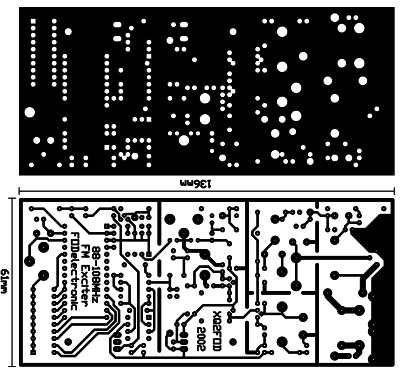 The
exciter is built on a double sided PCB, which has its top side copper left
mostly undisturbed as a ground plane. The copper is removed only around
non-grounded pins. The ground connections are soldered on the top side,
so it's not necessary to have plated-through holes.
The
exciter is built on a double sided PCB, which has its top side copper left
mostly undisturbed as a ground plane. The copper is removed only around
non-grounded pins. The ground connections are soldered on the top side,
so it's not necessary to have plated-through holes.
This drawing shows the two sides of the PCB, so that you can print it
and fold it in the middle to see how the two parts align. You will have
to invert the image to print it for making the board, so that the ink gets
in contact with the copper.
This PCB is fitted with soldered shields all around and between stages,
on both sides of the board. They are best installed before populating it.
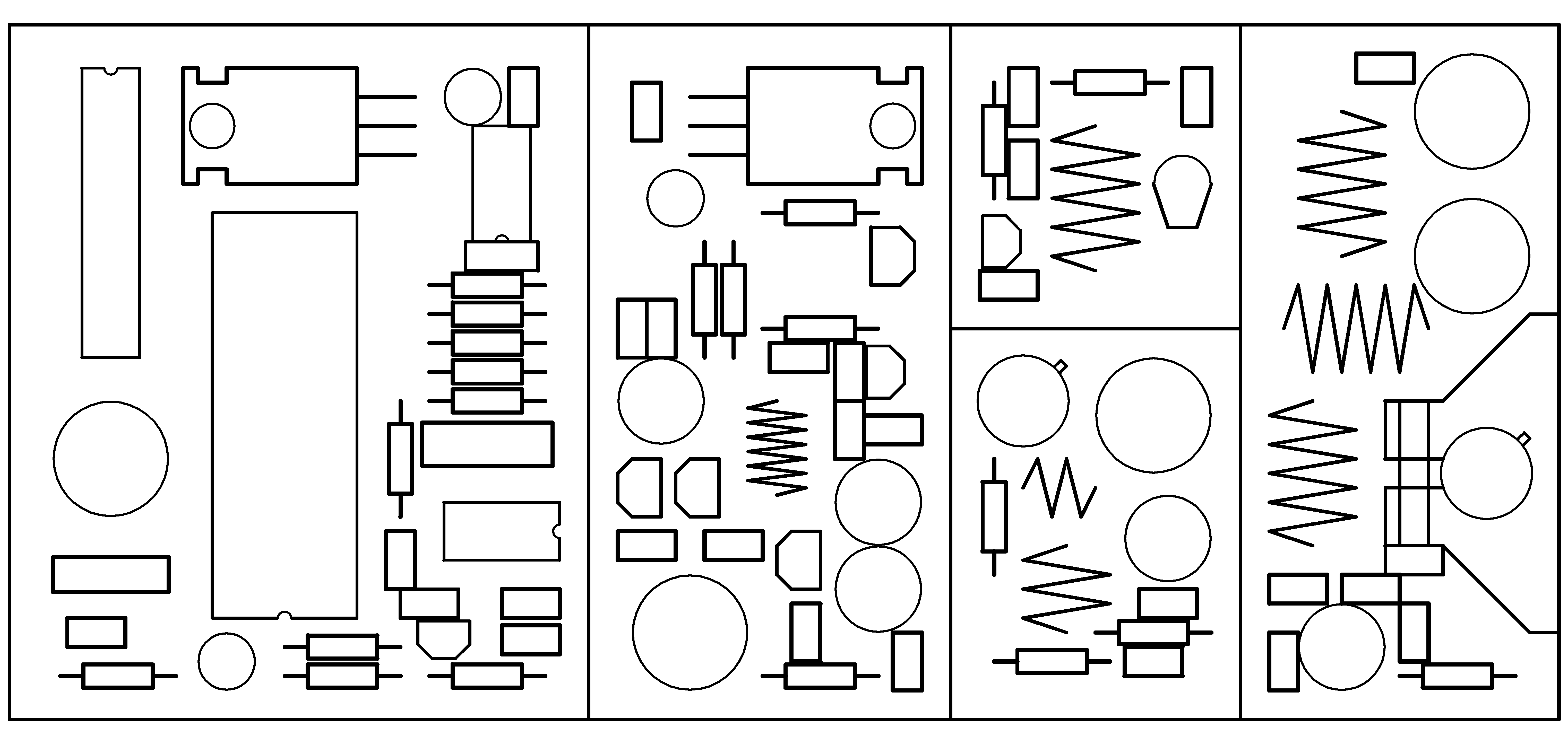
 This
image shows the parts layout. Again, you will have to find out which part
is which, using the schematic. It should be quite easy. Be careful, because
there is one component on the schematic that is NOT included in the board
design! It was added later, during debugging, and soldered under the board!
To make things more interesting and challenge you a bit, I will NOT tell
you which part that is! You will find out when you end up having one part
left over after assembling the board! :-)
This
image shows the parts layout. Again, you will have to find out which part
is which, using the schematic. It should be quite easy. Be careful, because
there is one component on the schematic that is NOT included in the board
design! It was added later, during debugging, and soldered under the board!
To make things more interesting and challenge you a bit, I will NOT tell
you which part that is! You will find out when you end up having one part
left over after assembling the board! :-)
The drawings of the coils are a reasonably close match to their actual
sizes.
 And this is how
the assembled exciter looks! You might notice the machined aluminium part
that encloses the output transistor. I made it on my hobby lathe. It's
a rather sophisticated way for connecting the TO-5-cased transistor to
an external heat sink! A simpler bracket will work as well. My original
idea was to stand this module on edge on a chassis or against a cabinet
wall, to use that as heat sink. Anyway, the circuit is so efficient that
the transistor barely needs an additional heatsink at all! I did
all testing without adding anything more than what's shown here.
And this is how
the assembled exciter looks! You might notice the machined aluminium part
that encloses the output transistor. I made it on my hobby lathe. It's
a rather sophisticated way for connecting the TO-5-cased transistor to
an external heat sink! A simpler bracket will work as well. My original
idea was to stand this module on edge on a chassis or against a cabinet
wall, to use that as heat sink. Anyway, the circuit is so efficient that
the transistor barely needs an additional heatsink at all! I did
all testing without adding anything more than what's shown here.
Many of the parts came from junked equipment. That includes the trimmers
and the dipped chokes. But compatible parts are available new. The crystal
was made by JAN Crystals. To order it, specify a frequency of 6.4000 MHz,
fundamental mode, parallel resonant, 30pF load capacitance, HC-49 holder,
with standard temperature, stability and tolerance ratings.
The output is connected via a BNC socket. All other connections go through
feedtrough capacitors. The shield is completed by push-on covers, made
of the same material used for the shield walls shown here. It's nothing
else than coffee tin cans, cut open and flattened! Some chocolates
and cookies also come in suitable cans!
Alignment of this circuit is not difficult. First you set all trimmers
to mid range and program the frequency. For this task, you simply add the
switch weights: The least significant switch produces 100kHz, the second
adds 200kHz, the next 400kHz, and so on, until the eighth, which adds 12.8
MHz. The ninth actually connects to two inputs of the PLL chip, so it adds
76.8 MHz, with the tenth switch adding 102.4MHz. To calculate switch settings
for a given frequency, you simply decompose it into its binary components,
and set the proper switches. Note that a switch that is ON is NOT adding
its frequency contribution! For example, if you want to transmit
on 96.5 MHz, you would set switches 9, 8, 7, 3, and 1 to OFF, the others
to ON. The full range of frequencies you can set in the synthesizer covers
the entire FM broadcast band and quite a bit more, but the rest of the
circuit was designed only for the broadcast band.
Now you should connect a 15V power supply to the main power input only,
with a voltmeter at the output of U3, and a frequency counter at the collector
of Q4. If you get the correct frequency, you are in big luck and should
go and play lottery! Usually the VCO will be out of capture range. If the
voltmeter reads around 14V, it means the frequency is too low. If it reads
close to zero, it means the frequency is too high. The frequency counter
should agree with this. You need to adjust the VCO center frequency to
bring it into range. For this task you have two adjustment points: One
is C20, the other is bending L4! Usually the trimmer alone does not give
enough range, so feel free to bend the coil. When you have adjusted the
VCO roughly right, the PLL will lock in, and you will get a stable output
frequency, very close to the one you want. Adjust L4 and C20 so that the
voltmeter reads roughly 9V. Such a relatively high varactor voltage is
convenient for best noise performance, because it keeps the varactors from
entering conduction at the RF peaks . Ideally you should adjust the coil
so that the trimmer is near center range with the voltage at 9V. This gives
you easiest correction later.
Now you can set the reference crystal to the precise frequency, by adjusting
C12 so that the frequency on the counter is exactly the correct one.
Let's go to the power stages: Connect an RF power meter and a 50 ohm
dummy load to the output, and apply a few volts to the variable voltage
input. Adjust C28, C32, C37 and C38 for highest power. If you run out of
range in any trimmer, correct that by bending the coils connected to it:
L5, L7, L11, L10. Now increase the voltage and retouch these trimmers.
You should get 4 to 5 watts output at 15V of supply voltage.
To avoid microphonic noises, after completing the adjustment you should
seal the oscillator coil, and maybe too the other air wound coils, with
bees wax or some other suitable material. Slight readjustment of
the trimmers might be needed after that.
Now you can connect the audio board to the exciter. Apply a 1kHz signal
to the audio board (both channels is best), strong enough to drive the
board into moderate limiting, and adjust R68 on the audio port to get +/-
75kHz deviation. If you don't have a deviation meter, you can get close
by hooking a scope to the audio output of an FM receiver, tuning it to
several local stations, note the audio levels produced by them, and then
tune to your transmitter and set its deviation to match that level. But
this system is very imprecise. It's best to get or make a real deviation
meter.
If you ever want to change the frequency, you have to reprogram the
dip switches and then retouch all trimmers, and possibly the coils, except
for C12, which should only require retouching after several years, when
the crystal has aged.
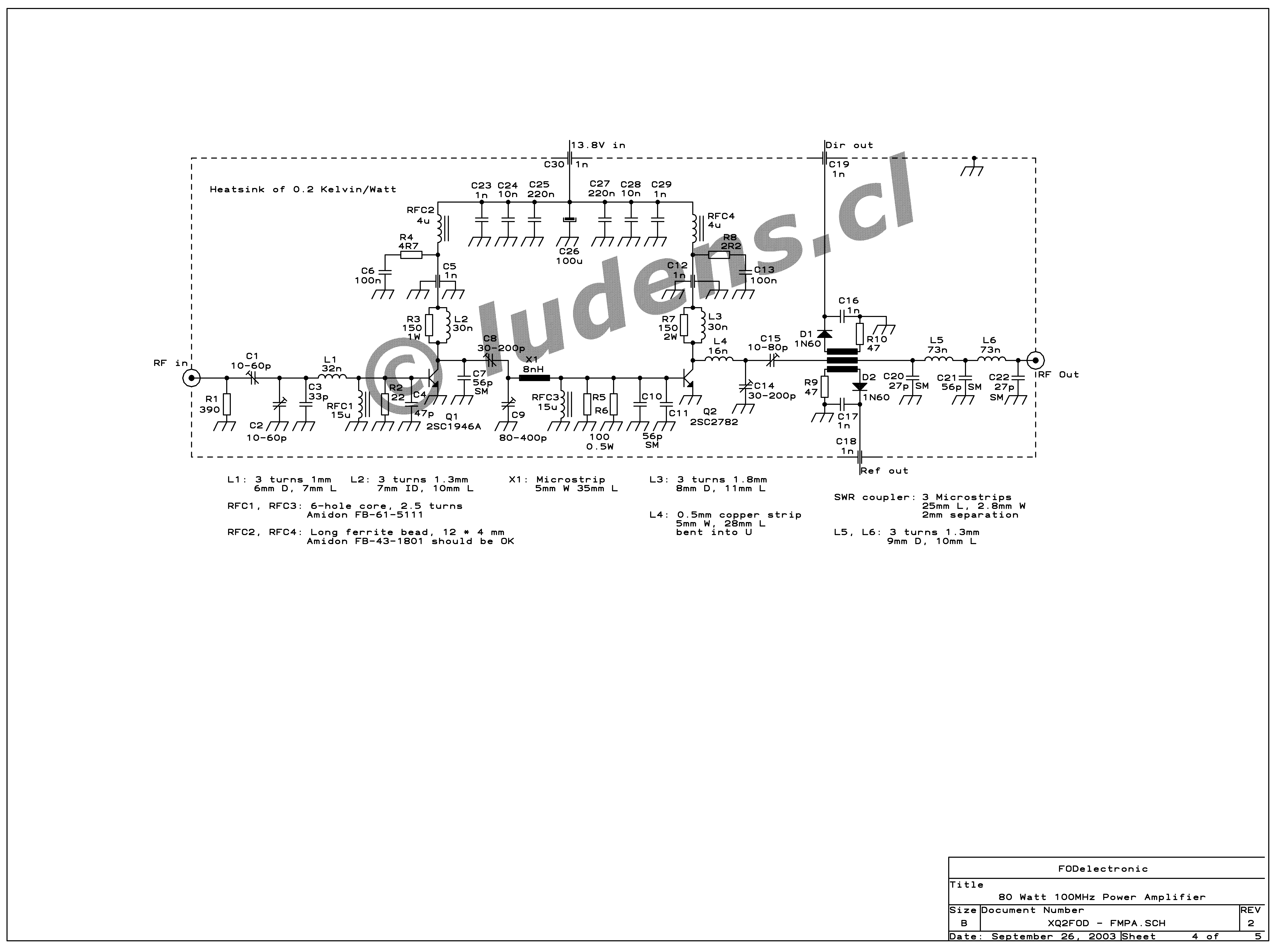
The 80 Watt power amplifier
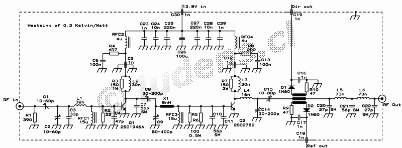 This
is a pretty conventional design, using bipolar transistors in a tuned class
C circuit. Thanks to the use of two stages, the amplifier can be driven
to full power with less than 1 watt driving power, so that a large gain
margin results in this transmitter.
This
is a pretty conventional design, using bipolar transistors in a tuned class
C circuit. Thanks to the use of two stages, the amplifier can be driven
to full power with less than 1 watt driving power, so that a large gain
margin results in this transmitter.
Bipolar VHF power transistors have a severe affinity for low frequency
self-oscillation. To obtain stability in this amplifier, I employed several
techniques, such as placing the resonances of base and collector chokes
far apart, damping the chokes with resistors, using RC combinations for
absorption of unwanted frequencies, using feedtrough capacitors for bypassing
on the board, etc. It took some tweaking, but the amplifier ended up unconditionally
stable.
The impedance matching network between the two transistors calls for
such a low inductance, that it would be impractical to make it with actual
wire. So I used a micro stripline etched on the PCB. Also, the power and
SWR sensor at the output was made with micro striplines.
Click on the schematic to get a full resolution version which also includes
detail about the micro striplines and other parts.
This amplifier has a low pass filter at the output, resulting in a signal
clean enough to be directly connected to an antenna. The SWR meter was
placed before the filter, in order to clean out the harmonics produced
by its diodes. In any case, while the signal is clean enough to easily
satisfy usual legal and technical requirements, this transmitter should
not be used at a multi-transmitter site without further narrowband filtering!
This is so because any other strong signals on nearby frequencies would
be picked up by the antenna and coupled to the power transistor, which
would mix it up with the own signal, creating a wide array of intermodulation
products, some of which would be re-radiated! This is a common and very
big problem in many multitransmitter sites. In such places, NOT EVEN ONE
transmitter should be allowed on the air without narrowband filtering!
Such filtering is easily accomplished by means of a single tuned cavity,
which can be constructed from copper tubing or sheet.
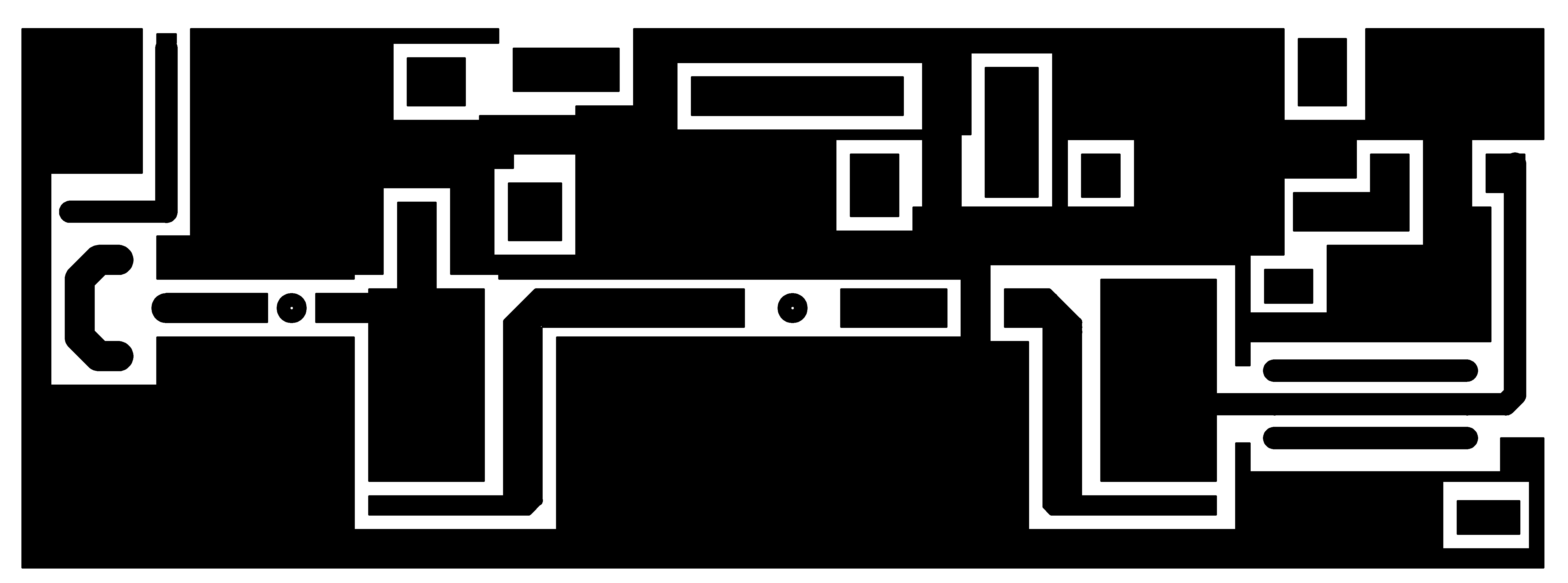
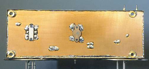
 Here
is the PCB layout, including the microstrips. The board is 20cm long and
is double-sided, with the backside being a continuous groundplane except
for two small pads at the driver transistor base and collector. I cut out
these pads with a knife, rather than making a whole computer drawing for
that!
Here
is the PCB layout, including the microstrips. The board is 20cm long and
is double-sided, with the backside being a continuous groundplane except
for two small pads at the driver transistor base and collector. I cut out
these pads with a knife, rather than making a whole computer drawing for
that!
 You
will have to drill and cut out the openings for the transistors. The power
transistor is mounted from above, while the driver transistor, due to its
small height, is mounted under the board. Both transistors are mounted
after soldering copper foils into the PCB openings, to join the upper and
lower groundplanes, and the driver transistor also has such copper straps
connecting the base and collector pads to the upper side of the board.
Here you can see how the transistors are soldered to the board, and the
spacers I used to give it the correct height. I first mounted the board
and transistors to the heatsink, then soldered the output transistor in
lace, then tack soldered the drive transistor's emitter leads from above,
through the opening, then again removed the board and soldered the driver
transistor fully. In this way the proper mechanical fit is assured. MAke
sure the transistor mounting surfaces are flat! My power transistor came
with a slightly rounded surface, so I first had to sand it flat! This is
critical for good heat transfer. Of course, use good thermal grease when
finally mounting the amplifier to the heatsink.
You
will have to drill and cut out the openings for the transistors. The power
transistor is mounted from above, while the driver transistor, due to its
small height, is mounted under the board. Both transistors are mounted
after soldering copper foils into the PCB openings, to join the upper and
lower groundplanes, and the driver transistor also has such copper straps
connecting the base and collector pads to the upper side of the board.
Here you can see how the transistors are soldered to the board, and the
spacers I used to give it the correct height. I first mounted the board
and transistors to the heatsink, then soldered the output transistor in
lace, then tack soldered the drive transistor's emitter leads from above,
through the opening, then again removed the board and soldered the driver
transistor fully. In this way the proper mechanical fit is assured. MAke
sure the transistor mounting surfaces are flat! My power transistor came
with a slightly rounded surface, so I first had to sand it flat! This is
critical for good heat transfer. Of course, use good thermal grease when
finally mounting the amplifier to the heatsink.
You can see that that there are also a few more places where things
connect through the board for best grounding. Of course, the shield around
the board also joins the two ground planes.
 And
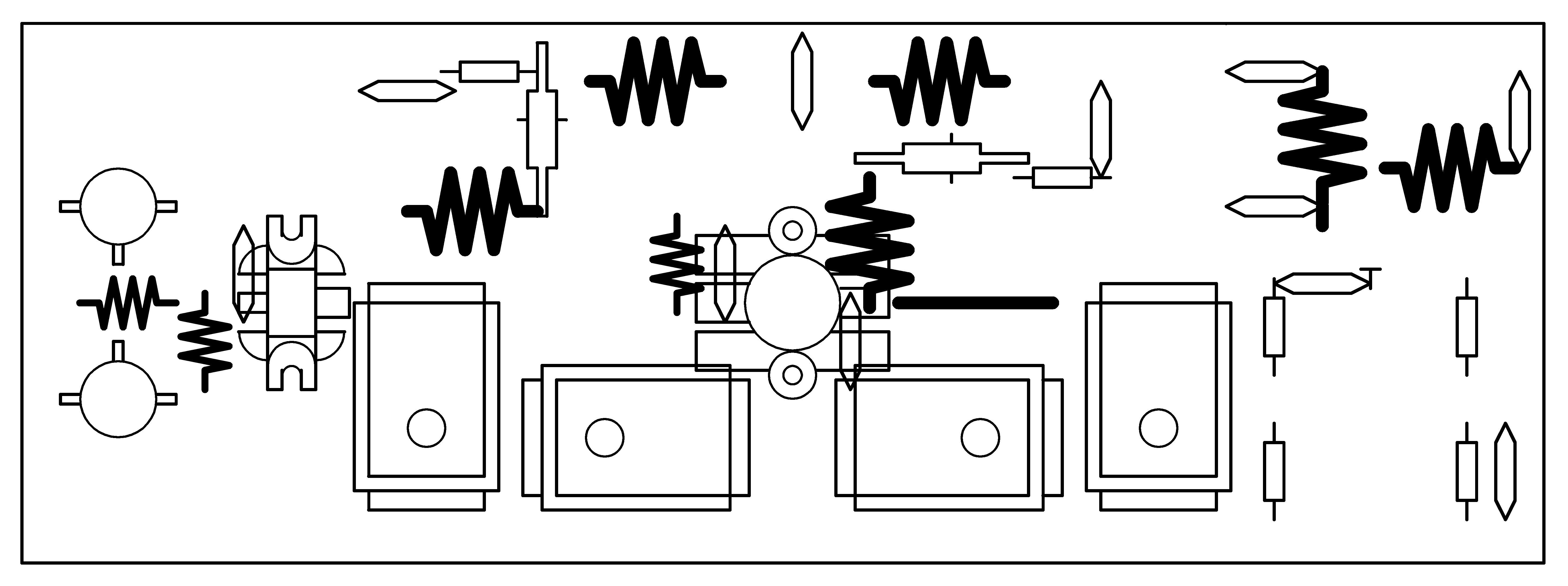
here is the parts overlay, as usual without parts identification!
And
here is the parts overlay, as usual without parts identification!
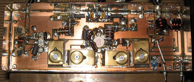 This is how the
complete power amplifier looks from above. You can see the striplines,
how the feedtrough caps (used as collector decoupling caps) are installed,
etc. Note the copper clad mica capacitors in the low pass filter at the
upper right.
This is how the
complete power amplifier looks from above. You can see the striplines,
how the feedtrough caps (used as collector decoupling caps) are installed,
etc. Note the copper clad mica capacitors in the low pass filter at the
upper right.
But let's better look in detail at some interesting areas:
 Here you can
see both transistors and the matching network between them. I couldn't
find trimmers that would stand the amount of RF current present in this
circuit! Every factory made trimmer I found would melt down! So I made
my own mica compression trimmers, using brass and copper sheet, brass base
plate, brass compression washer, and mica sheets originally intended for
TO-247 capsule mounting. All connections in the trimmers are soldered,
not just riveted like in many factory made trimmers. That solved the problem,
but even these trimmers get warm in use!
Here you can
see both transistors and the matching network between them. I couldn't
find trimmers that would stand the amount of RF current present in this
circuit! Every factory made trimmer I found would melt down! So I made
my own mica compression trimmers, using brass and copper sheet, brass base
plate, brass compression washer, and mica sheets originally intended for
TO-247 capsule mounting. All connections in the trimmers are soldered,
not just riveted like in many factory made trimmers. That solved the problem,
but even these trimmers get warm in use!
Note how the trimmers at both the input and the output of the power
transistor have their ground connections very close to the emitter leads.
 The output
matching network uses the same kind of trimmers. The one that appears in
the low middle of the picture is the one that takes the most current, more
than 15 amperes of RF! In continuous service, and at VHF where the skin
depth is very small, this is a large current. The same goes for the tank
"coil", which is made from a strip of 0.5mm copper sheet bent in "U" shape.
Despite its good thermal connection to the board, it gets hot enough to
become impossible to touch! Of course, anyway you shouldn't touch it while
the transmitter is on, because in addition to a heat burn you would get
an even nastier RF burn!
The output
matching network uses the same kind of trimmers. The one that appears in
the low middle of the picture is the one that takes the most current, more
than 15 amperes of RF! In continuous service, and at VHF where the skin
depth is very small, this is a large current. The same goes for the tank
"coil", which is made from a strip of 0.5mm copper sheet bent in "U" shape.
Despite its good thermal connection to the board, it gets hot enough to
become impossible to touch! Of course, anyway you shouldn't touch it while
the transmitter is on, because in addition to a heat burn you would get
an even nastier RF burn!
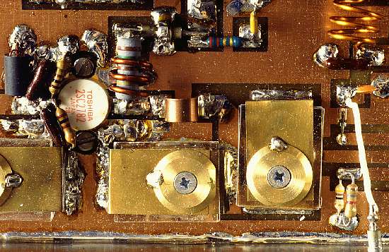
 A similar
problem happened with the capacitors for the output low pass filter. I
tried to use RF-rated dipped silver mica capacitors, as shown in the photo
above in its upper right corner, but they got so hot that they started
smelling! Surely their silver electrodes are too thin. They wouldn't have
lasted long in this service.
A similar
problem happened with the capacitors for the output low pass filter. I
tried to use RF-rated dipped silver mica capacitors, as shown in the photo
above in its upper right corner, but they got so hot that they started
smelling! Surely their silver electrodes are too thin. They wouldn't have
lasted long in this service.
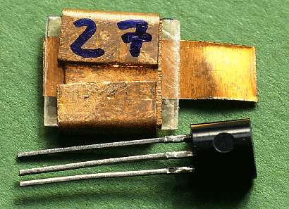
I didn't have any better RF capacitors on hand, and instead of ordering
heavy duty metal clad mica capacitors at several dollars each, I decided
to make my own. Here is one example, shown alongside a TO-92 transistor
for size comparison. I used 0.5mm copper sheet for the external electrode,
0.1mm copper foil for the inside one, and mica cut from TO-247 insulators.
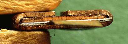 Here
is close-up edge-on look at one of my copper clad mica capacitors,
held in the jaws of a wooden clothes clip for the photo!
Here
is close-up edge-on look at one of my copper clad mica capacitors,
held in the jaws of a wooden clothes clip for the photo!
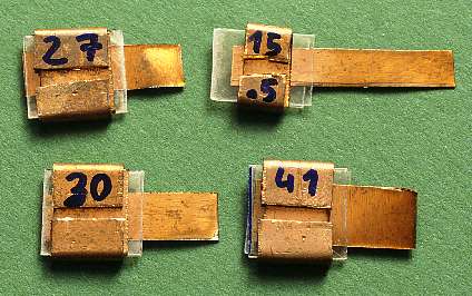 Since the thickness
of those mica insulators for semiconductor mounting varies a great deal,
making these capacitors is a cut and try process. I measured the
mica's thickness as best I could, calculated the surface necessary for
the capacitors, built them, and then measured them, using a test coil and
a grid dip meter. I wrote the value on each, and continued making capacitors
until I had some of values close enough for my low pass filter. The rest
I kept in stock for other projects!
Since the thickness
of those mica insulators for semiconductor mounting varies a great deal,
making these capacitors is a cut and try process. I measured the
mica's thickness as best I could, calculated the surface necessary for
the capacitors, built them, and then measured them, using a test coil and
a grid dip meter. I wrote the value on each, and continued making capacitors
until I had some of values close enough for my low pass filter. The rest
I kept in stock for other projects!
It's fun to notice that copper clad mica capacitors built in this way
perform just as good as factory made ones, that you can make any value
you need, and that they cost about 1% as much as the nice shiny branded
ones!
In the low pass filter, these copper clad mica capacitors get barely
warm. Since they are well soldered flat to the board, I don't know if they
conduct their loss heat into the board, or if they are only warmed up by
the filter coils! Because these coils surely do get warm in use, despite
being wound from very thick wire.
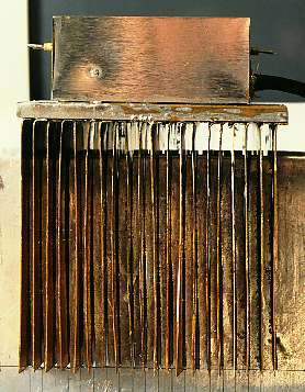 For
the tests I mounted the amplifier board on a rather large heat sink. It
consists of a 10 * 20 cm copper plate of 6mm thickness, to which I soldered
20 fins, made of 0.5mm copper sheet, measuring also 10 * 20cm each, having
L-shaped soldering edges. I made this heat sink some months before for
investigation purposes (see my thermal design page), and since it was lying
around, I used it. But with the total power dissipation of this amplifier
being something like 50 watts, a much smaller heat sink would be good enough,
if a small fan is used. Still, a copper heat spreader is a good idea, because
the power transistor is used at its maximum rating.
For
the tests I mounted the amplifier board on a rather large heat sink. It
consists of a 10 * 20 cm copper plate of 6mm thickness, to which I soldered
20 fins, made of 0.5mm copper sheet, measuring also 10 * 20cm each, having
L-shaped soldering edges. I made this heat sink some months before for
investigation purposes (see my thermal design page), and since it was lying
around, I used it. But with the total power dissipation of this amplifier
being something like 50 watts, a much smaller heat sink would be good enough,
if a small fan is used. Still, a copper heat spreader is a good idea, because
the power transistor is used at its maximum rating.
The results
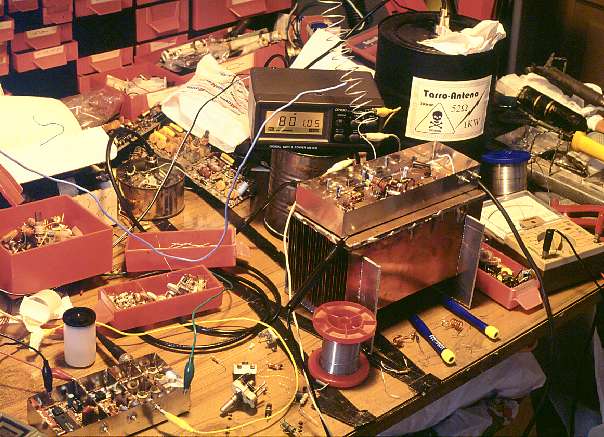 This photo shows
the transmitter being tested on my admittedly not very tidy workbench!
You can see the exciter in the lower left, and the amplifier with its overly
big heatsink standing on aluminium comb supports to avoid bending the thin
fins. There is my Aiwa power and SWR meter, and a large oil-can dummy load
to safely swallow the 80 watts (actually that dummy load can take a kilowatt
for a few minutes). An analog multimeter is showing the current, and the
rest are boxes of parts, tools, etc. The audio board ended up outside the
photo, along with the digital multimeter, frequency counter, oscilloscope,
etc. It was quite a mess, but worked very well!
This photo shows
the transmitter being tested on my admittedly not very tidy workbench!
You can see the exciter in the lower left, and the amplifier with its overly
big heatsink standing on aluminium comb supports to avoid bending the thin
fins. There is my Aiwa power and SWR meter, and a large oil-can dummy load
to safely swallow the 80 watts (actually that dummy load can take a kilowatt
for a few minutes). An analog multimeter is showing the current, and the
rest are boxes of parts, tools, etc. The audio board ended up outside the
photo, along with the digital multimeter, frequency counter, oscilloscope,
etc. It was quite a mess, but worked very well!
I ran several tests on the transmitter. One endurance test consisted
in running at 80 watts output for one week nonstop. No problems were noticed.
Other tests included temperature shifting, vibration (to check for microphonics),
varying the supply voltages, etc. The transmitter seems to be very well
behaved in every regard.
Then the qualitative tests were done. The stereo separation, measured
through my homemade FM receiver, came out as 52db. That's better than most.
The signal/noise ratio was beyond my measuring capabilities, which top
out at 82dB! That's better than almost anything one can hear from commercial
stations! The distortion was also too low to be measured, a result of the
careful balancing of the residual varactor nonlinearity with the effect
of series capacitance.
Then the ear test came! I hooked up my CD player, the transmitter, FM
receiver, amplifier and speakers, so that I could switch the sound forth
and back between the original signal from the CD, and the signal going
through the transmitter, a few meters of air (the radiation from the low
pass filter coils is much more than enough for this distance), and the
receiver. I played a CD by Roby Lakatos, the King of Gypsy fiddlers, which
I like a lot and which is great for testing because of its crisp,
clean and full sound. I was quite impressed by the fact that I could switch
forth and back between the original and the transmitted signal, without
detecting a difference by ear! So I'm happy to tell that this transmitter
preserves the full audible quality of a first-rate CD signal! The less
than perfect stereo separation is no issue at all, because no listener,
even in critical mode, can discern between 50dB separation, and perfect
separation!
The fourth module: To be done!
What is lacking to complete this transmitter is a fourth module, a quite
simple one, which should implement the following functions:
1) A DC-DC converter to accept the 13.8V nominal input and produce +/-
15V for the audio and exciter boards. This could be a standard 12V input,
factory made unit, or a homemade circuit.
2) A power control circuit. It should read the output power signal delivered
by the SWR/power sensor on the amplifier board, compare it to the setting
of a front-panel potentiometer, and adjust a pass regulator feeding the
last two stages of the exciter so as to set the output power to the desired
value. In addition. this circuit should implement protection functions:
It should reduce the power if the SWR signal exceeds a certain value, if
the temperature of the heatsink is too high (a thermistor or other temperature
sensor would be needed), and it should cut off the power altogether if
the PLL becomes unlocked, as indicated by the relevant signal coming from
the exciter. The power should be adjusted down fast, and back up slowly,
in order to have best protection.
3) Optionally the deviation could be monitored, sounding an audible
alarm signal or even cutting off the power if the allowable deviation is
exceeded.
Perhaps some day I get the motivation to build this fourth module, and
put them all into one box. If/when I do, I will finish this web page with
information about that module, and a photo of the completed transmitter!
Back to the homo ludens electronicus
page.
 The
two single-ended line-level audio signals enter through feedthrough capacitors,
and are welcomed by an LC low-pass filter to get rid of any RF that could
be on them. In each channel there is a buffer stage, and then a combined
pre-emphasis and soft limiter stage. The advantage of doing the limiting
and the pre-emphasis in one step is that it avoids overdeviating from loud
treble sounds, or having loud bass sounds flatten out the treble, without
the need of a multiband limiter. The gain of the non-limited portion of
the audio signals is adjustable by means of trimpots. Then comes a six-pole
low pass filter that removes signals above 15kHz.
The
two single-ended line-level audio signals enter through feedthrough capacitors,
and are welcomed by an LC low-pass filter to get rid of any RF that could
be on them. In each channel there is a buffer stage, and then a combined
pre-emphasis and soft limiter stage. The advantage of doing the limiting
and the pre-emphasis in one step is that it avoids overdeviating from loud
treble sounds, or having loud bass sounds flatten out the treble, without
the need of a multiband limiter. The gain of the non-limited portion of
the audio signals is adjustable by means of trimpots. Then comes a six-pole
low pass filter that removes signals above 15kHz.