The Power Jack 3500 Watt Inverter
Buyers beware!!!
 In late 2008 I needed to buy a high power true
sine wave inverter, for an alternative energy scheme. Scared away the
very poor quality I had seen too many times when asked to repair
Chinese inverters, but not willing to pay the outrageous prices asked
by manufacturers who are known for their quality products, I
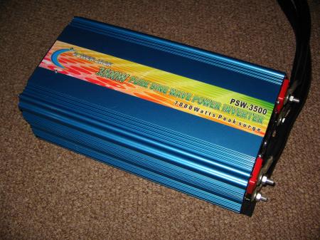
settled for a Taiwanese made inverter. It was the Power Jack PSW3500,
which is rated at 230V 50Hz output, 12Vdc input (at several hundred
amperes, of course!), 3500W continuous output, 7000W surge capability,
with a true sine wave output. In addition, it has a built-in 50A
charger, and the necessary detection and switch-over circuitry to make
it work as an UPS, if desired. The price seemed right, and Power Jack
made a lot of advertising telling that their product was much better
than the typical Chinese ones. I bought that, and I bought the
inverter. And I got cheated real good. It has often been said that one
gets what one pays for. Not so! I paid good, real,
decent money for this inverter, and got a piece of crap, if
you excuse the expression, which needed a complete re-engineering and
reconstruction to become usable.
In late 2008 I needed to buy a high power true
sine wave inverter, for an alternative energy scheme. Scared away the
very poor quality I had seen too many times when asked to repair
Chinese inverters, but not willing to pay the outrageous prices asked
by manufacturers who are known for their quality products, I
settled for a Taiwanese made inverter. It was the Power Jack PSW3500,
which is rated at 230V 50Hz output, 12Vdc input (at several hundred
amperes, of course!), 3500W continuous output, 7000W surge capability,
with a true sine wave output. In addition, it has a built-in 50A
charger, and the necessary detection and switch-over circuitry to make
it work as an UPS, if desired. The price seemed right, and Power Jack
made a lot of advertising telling that their product was much better
than the typical Chinese ones. I bought that, and I bought the
inverter. And I got cheated real good. It has often been said that one
gets what one pays for. Not so! I paid good, real,
decent money for this inverter, and got a piece of crap, if
you excuse the expression, which needed a complete re-engineering and
reconstruction to become usable.
I suffered the loss, and now at
least through this web page I'll get the satisfaction of
trying to help others not to fall in the same trap.
When my Power Jack inverter arrived, I read the
instruction leaflet, which is very brief, and shows how to hook it up,
in any of its three functions: As standalone inverter, as standalone
charger, and as UPS. I intended to use it only as standalone inverter.
I hooked it up, using very heavy wire for the battery connections.
After all, a 7kW surge will take almost 700 amperes from the battery
bank! I switched it on, and measured the output voltage, waveform, etc.
The voltage was fine, the waveform was a bit strange: One half
cycle of the sine wave was clean, while the other had about 20 volts of
high frequency noise riding on it! Also, the inverter produced an
impressive amount of radio interference, even with nothing connected to
the output! So much, that it completely erased all radio reception.
Input current consumption was less than 2 amperes, which seemed
fine. But the current was pulsed: Short, high current
pulses followed by pauses, averaging out to less than
2A. This is called "hiccup mode". I thought it was by design, so I
didn't worry. I did a load test, connecting a 2kW heater to the
inverter for just a few seconds, because my battery wasn't very good
and I didn't want to tax it too much. The output voltage
dropped a little, but not too much. All seemed fine. The
only really strange thing was that the LED power meter on the
inverter stayed fixed at 700 watts, regardless of how much power really
was being consumed! I ended the testing there, and wrote to
the seller, who told me that that was normal, and that the power meter
was there "only for show" (his exact words!). Oh well... I don't need a
power meter... And since the inverter arrived well and was working, I
gave the seller positive feedback (this was on ebay).
A few days later I wired up the whole system: A large,
good battery, the alternative energy system charging the
battery, regulated to 13.8V, the inverter, and connected it to feed my
house. There was very little consumption at that moment, not more than
10 watts or so. The inverter happily idled along, taking about 2.5A at
12V. I had to do some woodworking, so I went to get my tools, which
include a 1400W circular saw, a 600W planer, and a few more. When I had
everything set up and switched on the workbench light to start working,
nothing happened. Strange. I went back to where the inverter was, and
found the room full of white smoke, awful smell, the inverter giving
zero output, but still with its LEDs telling that all was fine: The
green "INV" LED was lit, the power meter bargraph was showing the
"normal" 700 watts, and the battery voltage meter was at 13V. But no
output, and lots of smoke... The nice shiny new Power Jack inverter had
commited suicide, while running at almost no load, whithin the first
two hours of operation!
 I first contacted the seller again, telling what had happened. Since he
took some time to reply, in the meantime I opened the inverter, to have
a look at the damage.
I first contacted the seller again, telling what had happened. Since he
took some time to reply, in the meantime I opened the inverter, to have
a look at the damage.
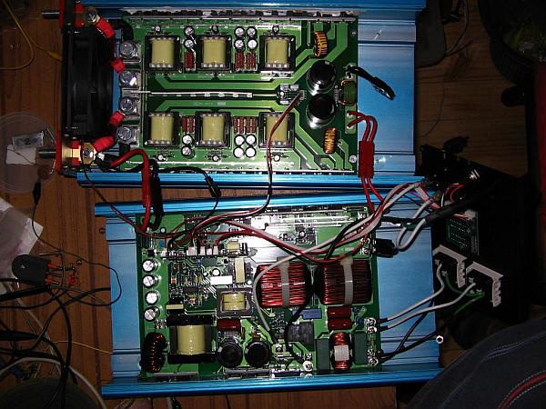
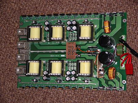
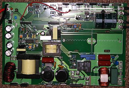
The shell comes apart in two halves. The bottom half, shown in
the upper place here, contains just the power components of the
push-pull DC-DC converter, which steps up the 12V to about 340V or so.
It consists of six converter groups, each having a transformer, two
pairs of MOSFETs, and assorted driving, bypassing and snubbering
components. The secondaries of the transformers are connected
in series in two groups of three. Each group has a bridge rectifier,
and an LC filter. The outputs of the two groups are connected in
series. No voltage balancing is employed at all. And there is no
current sensor whatsoever!
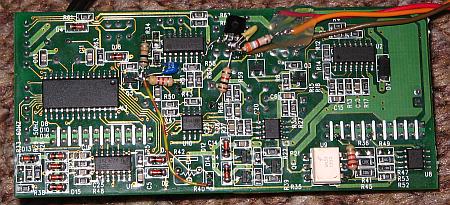
The other big board is what I will call the mainboard. It
carries the sine wave chopper, which uses an IGBT bridge, and an LC
output filter with two big inductors. There is also the charger
circuit, all the switchover system, and a plug-in control board, which
controls the DC-DC converter, the switchover, the
charger, and drives the chopper.
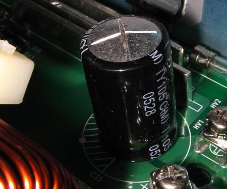
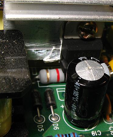
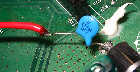
I immediately noticed two popped electrolytic capacitors, one
of which you can see in this photo. It's a 100uF, 400V capacitor, which
is THE ONLY capacitor across the high voltage DC bus on the sine wave
chopper board! It has to take the full high frequency ripple current,
which can easily be several amperes. And the ripple current rating for
such a capacitor is not over one ampere. Was that the reason for it
popping open?
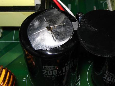
And here is the other one. This is the filter capacitor used
in one of the two series-connected rectifier/filter group, that produce
the high voltage DC. Its companion was still fine, it seemed.
At this point, it looked like some big overvoltage had
happened, lasting a good while, because electrolytic caps don't pop on
short overloads.
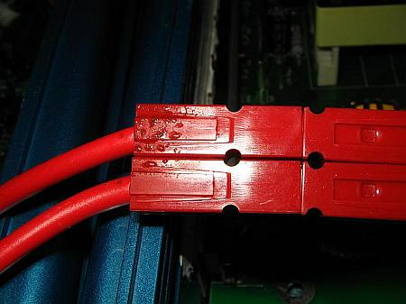
This is one of the connectors linking the high voltage DC from
the converter board to the main board. It has spills of capacitor juice
on it.
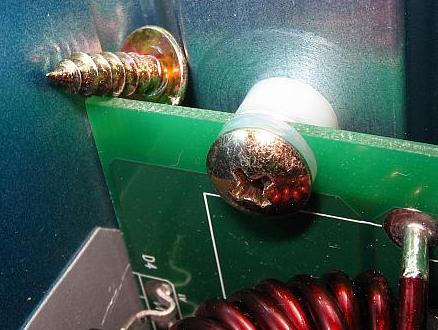
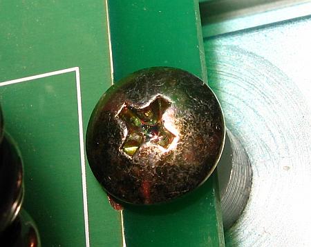
As I looked more closely, I started finding more and more
horrible things! Here, for example, is a screw, that came loose during
shipping, and got caught in this place. Having been caught, at least it
didn't cause any short circuit. But screws coming loose inside
equipment are a very bad thing!
Here is a spacer, that came loose when its screw fell out. The
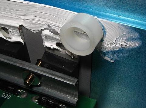
spacer got stuck in the white thermal grease, and stayed put there.
Hmm... why is there any thermal grease at all? There is a
silicone rubber pad between the power components and the heatsink! This
makes thermal grease unnecessary, one would think!
After picking off the spacer, and looking more closely, it
became clear: The pressure bar holding these parts against the heatsink
was installed much too low, pressing down only on the lower edge of the
TO-220 parts! As a result, these lower areas get buried in the
soft rubber, and the tops of the parts stick out in free air, with no
thermal contact whatsoever!
Instead of fixing the problem, Power Jack "engineers" chose to
smear thermal grease all over the flanges! If at least they had smeared
the grease INTO the voids, that might have worked, at least a little
bit, but smearing the grease OVER the parts and rubber pad is
totally useless.
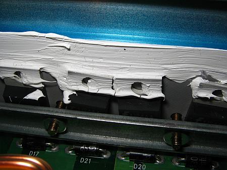
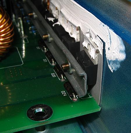
And here is yet another photo showing how these people tried
to solve the problem of lousy thermal contact! There is not a trace of
grease between the parts and the rubber. There is just air there. The
grease is outside the voids.
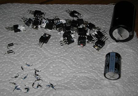
I then did the complete troubleshooting, and found that all 24
MOSFETs were burned, with the sources open and the drains shorted to
the gates. The fuses were fine, thank you. Along with the MOSFETs, the
24 gate resistors also failed. Then there are the two popped
electrolytic caps, and also two overvoltage protector diodes (transil).
These failed in short circuit, on the side where the capacitor still
was fine.
Since it was too expensive to ship the inverter back to Taiwan
for repair, and then again to Chile, and the whole
import/export would be a real hassle, to avoid paying the import taxes
a second time, I proposed that Power Jack simply sent me the required
spare parts. They agreed, and sent them very quickly. So I
proceeded to disassemble much of the inverter, and replace the bad
parts.
At this point, at least part of the failure mechanism became
clear: For some reason the DC link voltage had soared to a far
excessive value, and for a good time. For that reason, the capacitors
popped. But popped capacitors typically keep working for
a while! So did these. When the voltage soared further, one of
the overvoltage protectors must have failed from stress, while trying
to absorb those pulses. It created a short. This overstressed and
shorted the other protector, so that now there was a dead short across
one set of three transformers. Since there is no current
sensing whatsoever, this took out the MOSFETS of that side, before the
fuses could react. And the 12V leaking back from the bad MOSFETs,
through the shared drive circuitry, to the other three converters, put
those MOSFETS into continuous conduction, taking them out just like
their companions. An uncontrolled chain reaction like the worst.
Fortunately it wasn't nuclear! And the control circuit, dumb and
uninformed as it is, didn't notice a thing, and displayed on the LEDs
that everything was fine! Is that poor design? What do you think?
With the new components installed, the inverter again worked,
but I was hesitant to use it like that. It would have burned out again
very soon. Instead, I stored it away, and spend the next several months
doing more important work, using a stinky and noisy gasoline powered
genset instead of the inverter. So much for alternative
energy. At least the genset works.
But in July 2009 I took up the inverter again. I decided to
completely check it up, understand it in detail, and cure all its
problems, before daring to use it again. And here started one of the
most frustrating episodes of my career as electronic engineer! I
learned that when a design is bad, it is BAD, really,
and when you think you have found all the bugs, and can start fixing
them, you find even more!
Instead of continuing to tell the story in chronological
order, I will list the flaws, one by one. That will take a lot of time
and space, I assure you.
Lack of current sensing in the DC-DC converter:
Normally any switching converter uses current sensing. The
better converters employ the current sensor to limit the pulse width on
a cycle-by-cycle basis. This allows fast, precise and safe control of
the current flowing through the system. Simpler systems do not use
cycle-by-cycle limiting, but at least they sense the average current,
and reduce the duty cycle when the current is reaching the acceptable
limit, to avoid burning out components if something abnormal happens.
The Power Jack inverter has none. If this is due to cheapness or
incompetence, I don't know.
Unstable control loop:
The DC-DC converter in this inverter uses an SG3525 control
IC. Its error amplifier was configured as a plain,
simple integrator: A single capacitor as the feedback path.
This results in the error amplifier having a constant -90 degree phase
shift. But in the power section of the DC-DC converter, the dominant
elements are the filter capacitance, and the input source resistance
(batteries, cables, MOSFETs, transformers), giving the power system
also a -90 degree phase shift throughout the low frequency range! This
adds up to -180 degrees, which together with the inverting nature of
any control loop produces in-phase (positive) feedback. In
this case the positive feedback happens from less than
10Hz to over 1kHz. The limits vary depending on the
load on the output, which is the third element influencing the power
circuit's response! The filter inductance comes last in order of
importance. It's much too small to have any significant effect.
With positive feedback, and positive loop gain, the stage is
set for self-oscillations to occur. And this was the cause of the
hiccupping I noticed. It was NOT by design. It was by poor
design!
The control loop is unstable under almost all load
conditions, resulting in the inverter drawing extremely high current
pulses, followed by pauses, with the frequency and duty cycle given
mostly by the load on the output. I measured pulses in the kiloampere
range and millisecond duration, while the average current was
just a few tens of amperes!
Flux walking:
Push-pull converters like these are prone to core saturation
and consequent failure from flux walking. To make sure no damaging
saturation will happen, the only way is to use pulse by pulse current
limiting - which wasn't done in this inverter. Another method, not 100%
safe but good enough in most cases, is making the error amplifier so
slow that the lengths of subsequent pulses cannot change much,
and then rely on the MOSFET's and circuit's resistances to balance out
any remaining asymmetry. This was also not done in this
inverter! The error amplifier has a gain bandwidth product close to
20kHz! As a result, this circuit is prone to core saturation and MOSFET
destruction whenever there is significant coupling of the signal on the
transformers into the feedback loop!
Inadequate filter chokes:
The high voltage filter uses two filter chokes,
each consisting of 30 turns wound on a yellow and white toroid
about 27mm in diameter. This seems to be an
Amidon/Micrometals T-106-26, or an equivalent. Assuming it is the
mentioned type of toroid, the inductance would be 81uH while the
current is low. But the highest current these chokes
have to take, at the waveform peak when a 3500W load is connected, is
21.5A, and at this current level the cores are already
deep into saturation, with their effective permeability being
about 1/4 of the original value, and the inductance having dropped to
just 20uH! And at the rated 7000W surge power, the situation is even
much worse.
This is just the beginning of the problem. At 81uH,
the ripple current in these inductors is 16A p-p, which would be
roughly 6A rms. This ripple current will theoretically increase to 24A
rms, or well over 118A p-p, at full load! It follows that
this DC-DC converter never enters
continuous current mode operation at all! It's always in
discontinuous mode, with the peak current in the
diodes, MOSFETs, etc, over twice the average cycle current! In
reality, at 21.5A output current, the inductor current will be swinging
between zero and about 50A all the time, which means a peak current of
over 160A in each single MOSFET, plus any magnetizing current for the
transformers!
I leave it to the imagination of the reader to guess how long
the filter capacitors will live, when they are subjected to an average
of maybe 15A of ripple current, while their total combined ripple
current rating is about 4A maximum.
A quick calculation shows that these poor toroids have to work
at an AC flux density of 0.35 Tesla. And this doesn't change very much
over the power range. Even at a relatively low load power, the AC flux
density is already almost that high, and it remains there, as the
current continues to increase, while the cores increasingly
saturate. The problem is that this high AC flux density, at the high
frequency this converter operates on, produce a whopping 53 watts of
power loss in each core! That's enough to make these coils unsolder
themselves from the circuit, and probably to burn the insulation and/or
meet the Curie temperature!
While testing the inverter at very low power (just 100 watts,
less than 3% of the rated output), where the inductors are not yet
close to the full AC flux density they reach at higher powers, in a
matter of one minute they got too hot to touch, and after
five minutes they started discoloring, and smelling burned!
To operate correctly, this inverter needs toroidal cores many
times larger than these, so that they can be wound to provide a few
hundred microhenries, and not saturate until at least 50A, to
enable them to handle the rated 7kW surge load too. This would
also make them work at much lower AC flux density, producing acceptable
power loss and heating. Alas, Power Jack in Taiwan
was too cheap or inept to do that.
Optoisolator drift:
The feedback signal of the DC-DC converter comes through an
optoisolator, to afford the required galvanic insulation between the DC
link, which is at output line potential, and the control circuit, which
is at battery potential. In principle this is fine. The problem is that
the designer of this inverter apparently didn't know that optoisolators
have a strong temperature coefficient! When they warm up,
their current transfer rate goes down markedly. And in this
Power Jack inverter, the optoisolator is used in such a way that its
drift directly affects the "regulated" DC link voltage! As the
optoisolator warms up, the DC high voltage goes up, and up,
and up, and.... BANG! This is one very
likely trigger for the chain reaction that burned out my
inverter before two hours were over! To compound the problem, this
optoisolator sits in the top of the case, in a pretty warm
spot.
Unsafe feedback:
Good design practices dictate that circuits should be made so
that in the event of a malfunction they will shut down without further
damage, whenever possible. Unfortunately the Power Jack inverter is
made in the opposite way. The control loop uses an auxiliary power
supply, which is derived from another auxiliary power supply, both of
which use SMT components stressed beyond their absolute maximum
ratings. Specially the ripple current rating of the small electrolytic
caps is far exceeded. And if any of these two auxiliary power supplies
fails, the feedback loop is broken, in such a way that the DC
high voltage will soar far above the capacitor and transient protector
ratings. BANG!
Also, the high voltage is sensed through three tiny SMT
resistors in series. Each of these resistors is rated at 100mW. One is
360k, another 200k, and the third is just 20k. The DC voltage
is about 340V. This results in a total power dissipation of 200mW. If
the three resistors were of the same value, this would mean 67mW on
each, which is a bit tight for comfort, but OK. But with the
values used, the 360k resistor works at 124mW, well above its
absolute maximum rating! If it fails, the feedback loop is opened, the
voltage soars, and BANG!
Selecting such different values for the three resistors in
series is not a matter of cheapness. It's plain, simple, gross
incompetence.
Optoisolators are less prone to failing, and this
one is used in the low area of its rating, so it should be
pretty safe. But anyway, if it fails open, which is the most
common failure mode, BANG, again!
Lack of overvoltage protection:
The unsafe feedback loop, using an optoisolator so that it
causes severe voltage drift, would in itself warrant the inclusion of
an independent overvoltage protection circuit: Anything that in the
event of the voltage rising to a value that is
dangerous to the inverter or to the devices powered by it,
would activate a safe shutdown mechanism. But in this inverter, there
is even more reason to use it: The filter capacitance on the DC link is
so small, that even a quite moderately reactive load on the output
would drive up the voltage on the DC link to a dangerous level! Sure, a
cheap inverter doesn't HAVE to handle highly reactive loads. But if the
load is too reactive to handle safely, it should shut down, instead of
exploding! Well, this one explodes. It would be simple to include an
overvoltage detection circuit that shuts down the inverter in the event
of overvoltage. This would provide protection both in the event of a
control circuit problem, or an overly reactive load. And on top of all
that, don't forget that this inverter's DC-DC converter has two
sections connected in series, and each of these sections consists of
three converter units, and each of these six converters is individually
fused! If the fuse for just TWO converters open from overload, which is
a perfectly feasible scenario, the DC-DC converter would end up badly
unbalanced, with one group providing 3 times as much voltage
as the other. With the total voltage regulated to 340V, and each filter
capacitor rated at 200V, this would cause 255V to show up on one of the
200V capacitors: BANG! But no, despite all this, Power Jack
people were too cheap to include any overvoltage shutdown. The
necessary components to afford full protection cost about two dollars.
Not including them is either being outstandingly cheap, or
being incompetent.
Nonsensical output filter arrangement:
This inverter uses an H-bridge of four IGBTs, with pulse width
modulation at 20kHz, to produce the sine wave output. The output filter
consists of two really large toroidal inductors, and two film
capacitors. All this seems good and fine to me. But when looking at the
board, which you can see in the first photo on this page, I would never
have thought that The Power Jack engineers chose to place BOTH
inductors on the SAME side of the bridge's output! Of course, on a
piece of paper, it doesn't matter whether both are on the same side, or
each on one side. Electrically, they end up in series anyway. In
practice, however, it makes a whole world of a difference, in terms of
interference to other devices! As it is in this inverter, one side of
the chopper appears directly connected to the output, and the negative
side of the DC bus is capacitively coupled to the negative of the
battery. This results in 340V of square wave 20kHz riding on the output
during one semicycle, relative to the battery circuit, which is
typically grounded! Talk about a big noise bomb!
And yes, there is an EMI filter in the output line.
Unfortunately, it is configured the wrong way, and so it's completely
useless: The small ground bypass capacitors were installed on the side
of the filter that goes to the chopper, rather than on the output side!
They surely blew up when at the lab they actually connected
them to ground, because that results in a powerful 340V 20kHz
signal connected straight to two little ceramic caps: The one
from the "hot" bridge side to ground, and the one from the
negative DC link side to ground!
Do you want to know which was Power Jack's solution to this
problem? Simple: They left the ground connection of the EMI filter
disconnected!!! The result: Absolutely impressive,
all-overwhelming radio interference! This is particularly bad because
many people buy sine wave inverters to feed sensitive studio audio
equipment, or laboratory instrumentation, with a clean AC supply! Ha ha!
Risk of death by electrocution!
I wouldn't have written this web page bashing on Power Jack,
if their product was simply unuseable. But when I noticed the gross,
extremely dangerous blunter they did by joining the AC input to the
output, I decided I had to write this page! I hope that nobody has
been electrocuted yet by one of these inverters!
As explained in the beginning, this inverter includes a
battery charger, and switchover circuitry for UPS (Uninterruptible
Power Supply) service. So there is an AC input and an AC output. The AC
output is switched between the AC input, and the inverter output, and
in addition the AC input goes to the charger. So far, so good. The
problem is that the geniuses at Power Jack chose to use a single pole
relay to switch just ONE side of the 220V line, while the other side of
the 220V remains connected at all times, to the input, output, charger
and inverter! As a result, when using this thing as a
standalone inverter, one of the 220V output poles is fully
exposed at the male AC input plug!!!
The concept of this was probably to use this permanently
connected side as the neutral, but that doesn't work out, because the
input and output connections don't use polarized connectors. The output
universal jacks can be connected in any polarity, while the input
connection comes from Taiwan just as a stripped wire, to which the user
has to install a plug of the kind used in his country. And the manual
has not even one word of warning about phase, neutral and the like!
So it's perfectly possible that someone connects this inverter
to his house, leaving the input disconnected, and uses a standard plug
to mate with the jack on the inverter. The house wiring will normally
have the neutral grounded. Depending on which way this plug
is put in, one pin of the inverter's 220V input plug will have either
the neutral, or the phase on one of its
pins, exposed for anyone to touch!
Folks, this is more than being cheap, or being incompetent: It
wouldn't be hard for a lawyer to bring up charges for attempted
manslaughter, or, if someone actually gets killed, erase the word
"attempted"! I can only hope that each of these Power Jack
inverters burns out quickly enough to become "safe", before
getting a chance to kill anybody. And I'm glad I didn't touch the
exposed male plug on mine, in the short while it worked!
After this major scare, let's go back to what may look like
petty issues.
Lack of EMI filtering in charger:
The charger is a simple half-bridge circuit. It follows the
trend of crappy Chinese PC power supplies, and has absolutely no EMI
filtering whatsoever! The AC input goes via an inrush current limiter
directly to the rectifier, filter caps, and from there to the IGBTs. As
a result, the charger causes severe radio interference. Not as brutal
as the one the sine wave chopper causes, but still
severe enough to disrupt HF and MF radio reception, and even cause
strong "snow" on a VHF TV.
Instability of the charger's control loop:
 The control circuit for this charger has both
voltage and current regulation, which is fine. The problem is that the
control loop is misdesigned, resulting in instability when operating in
current-limited mode. The charger pulses heavily, and if left doing
that for long enough, it would fail. It requires re-design.
The control circuit for this charger has both
voltage and current regulation, which is fine. The problem is that the
control loop is misdesigned, resulting in instability when operating in
current-limited mode. The charger pulses heavily, and if left doing
that for long enough, it would fail. It requires re-design.
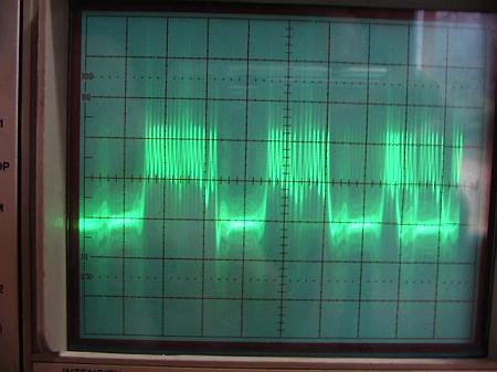
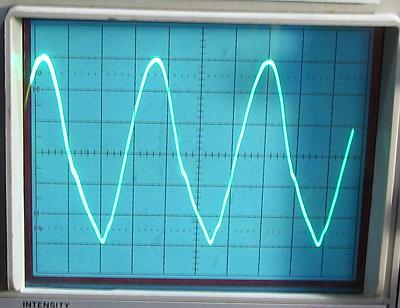
Here you can see an oscillogram of the charger's output
voltage. The main square wave happens at about 160Hz, and the triangle
wave on the upper side of the square wave is at roughly 3kHz. The "fog"
around the waveform is noise fed through from the main 100kHz switching
process. As you can see, the charger's control loop oscillates
at two frequencies at the same time, with some modulation on each, and
on top of that there is about a half volt of switching
frequency noise! How's that for crappy design?
It looks like the designer copied the control loop from some
application note or other source, without understanding it,
and not realizing that it was meant for a power supply, not for a
battery charger with its immense de-stabilizing "capacitive" load
attached!
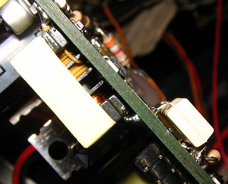
Poor design of the thermal attachment of the power components.
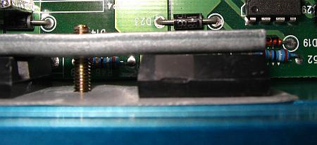
Near the beginning of the page I showed you photos of how the
TO220 cases were mounted such that their tops separate from the thermal
pad, and how these people smeared thermal grease over it, in a vain
attempt to fix the problem. Well, here is a top-down view of one of the
larger parts. These have their mounting bars at the proper height, but
use just one tiny screw in the middle to press down two big components.
Before having any chance to apply enough pressure, the bars bend, and
apply pressure only to one edge of the part! The result: Very poor
thermal contact, because a big portion of the part's seating surface
ends up with a layer of air between it and the heatsink!
You can see the the board through the wedge gap between the
pressure bar and the part!
And one more problem: Even electronic hobbyists, let alone
engineers, know that power devices first must
be mounted to the heat sink, then
soldered to the circuit board! This inverter is designed the other way
around. There is no way to solder the parts once installed on the heat
sink. It becomes necessary to solder them first, and then install the
whole board with all the parts in the case, and bolt down the parts as
the last step! This results in poor seating, and severe mechanical
stress on the connection pins.
By the way: The DC-DC converter board, with its heavy
transformers, has no mounting screws whatsoever. It's attached ONLY by
the pins of the TO220 MOSFETs and diodes!
Oh, and while we are looking at the cooling, let me tell you
that the case of this inverter, which acts as the only heatsink for the
big power semiconductors, has the fins on the outside,
in horizontal orientation, while the fan draws
air through the inside, where there are no fins!
Not that this would matter much, because anyway the fan
is essentially decorative: The openings through which air can enter
the inverter have a total combined area of less than 5% of the
fan's area!
Lack of creepage distance:
It is required by safety standards to leave a certain distance
between printed circuit tracks that carry high voltage, in order to
prevent creepage, flashover, and the ensuing risk for people, or
damage. At usual line voltages, 4 millimeters is a decent distance.
Well, this inverter in many places has just 0.8 mm clearance. In the
photo above, you can see how close the PCB comes to the case. Whether
it touches, or if a small amount of air remains between, depends mostly
on luck. The tracks carrying high voltage go to about 1mm of the board
edge, and in one place, apparently due to lax manufacturing tolerances,
the tracks almost reach the edge.
The same meager creepage distances are kept to the screw
holes. Insulating washers were used to keep the screws from directly
touching the copper areas, but the copper reaches very, very close to
the screw holes, and thus to the screws, which thread into the
aluminium enclosure.
I grinded away some copper in the most dangerous places, to
regain some peace of mind.
Wrong component choices:
When I first tried the charger included in this inverter, the
filter capacitor of the charger's auxiliary power supply quickly got
hot and bulged out. I noticed it just in time to avoid another
capacitor explosion and electrolyte spillage! It's a 470uF 35V
capacitor, which works at well above 35V...
The bad choice isn't the capacitor, but the transformer
feeding it. There is no reason to use such a high voltage, to feed a
7815 regulator chip. Fed from that high voltage, the regulator gets
very warm too.
By the way, the rather largish heatsink on this regulator is
supported SOLELY by the regulator! It has no other attachments
anywhere! It's a rather wobbly affair.
And also it's interesting to note that the heat coming from
this heatsink flows directly to the optoisolator, whose warming causes
the "regulated" high voltage to drift up! So, if the unit is used as an
UPS, the optoisolator will be hot whenever the inverter comes in, which
will make the inverter produce a very high voltage.
What do you do if a large stranded wire doesn't want to thread
through the hole in the printed circuit board? Simple solution, Power
Jack style: You cut off half of the strands, and use only the remaining
ones!
Shall I continue? I could name quite a few additional flaws!
But this page is getting too long already.
Recovery attempts
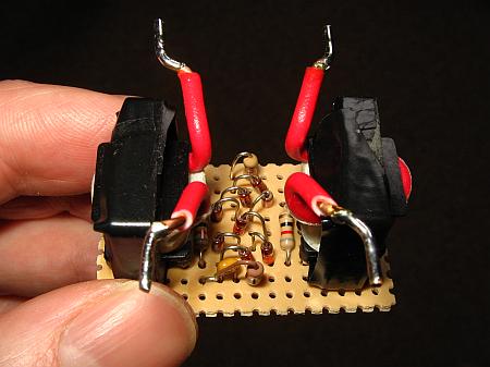
To reduce the risk of burning out all the power
semiconductors again, the first thing I did was adding protection
circuitry. Shown in this photo is a current sensor, that uses two
current transformers, each with a load resistor and a bridge rectifier.
They sense the current on each group of secondary windings of the DC-DC
converter. The outputs are in parallel, so that the highest one will
dominate.
I would have preferred, by far, to sense the primary current,
but the board layout didn't lend itself to it. It would have required
essentially making a new printed circuit board. So I decided to try my
luck with this secondary side current sensor.
I installed this current sensor on the DC-DC converter board,
and also installed there an overvoltage protection circuit.
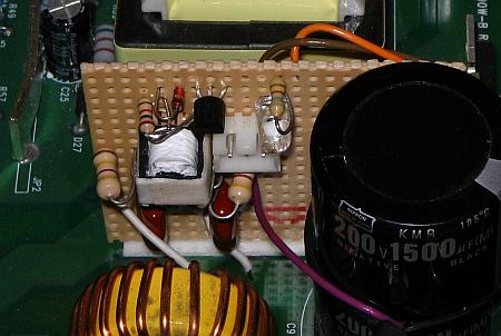
This overvoltage protector senses the voltage on each of the
1500uF 200V filter capacitors separately, and if any of them exceeds
180V for a significant time, it triggers a small SCR, which is used to
shut down the DC-DC converter, and light a red LED. The circuit is
reset when the inverter is switched off and on again. This is
the protection circuit cited somewhere up in this page, that costs
less than two dollars. It works with DIACs, that form a
relaxation oscillator around a tiny ferrite transformer, which triggers
the SCR.
Note that both the current sensor and the overvoltage
protection circuit are galvanically insulated from the
circuits they sense!
In the foreground you can see one of the yellow toroidal
cores, which are much too small, and get extremely hot. This one
already has black burn marks on it!
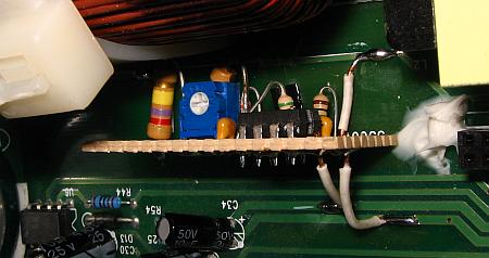
Then I moved the error amplifier to the other side of the
optoisolator, to eliminate almost all effect of the optoisolator's
thermal drift. To do this, I had to build a new error amplifier, and
install it on a small board, because on the control board I had too
little room to install anything. This error amplifier contains a high
voltage divider using two 270k, 1/2 watt resistors in series. That's a
lot safer than the original ultra-tiny and overloaded SMD divider!
While doing this, I also inverted the function of the
optoisolator. As a result, if it fails now, the output voltage will go
to zero, and if any of the auxiliary supplies fails, the voltage will
too go to zero.
The control board was modified, to eliminate the SMD high
voltage divider, buffer, and the original error
amplifier (which used the internal amplifier of the SG3525), and
add a few parts needed to inject the signal from the
optoisolator directly into the pulse width modulator, and to provide an
injection point for my current sensor and overvoltage protector.
Then I got my Dremel out, and severely cut up the main board!
I rearranged the chopper's output filter so that now there is one
inductor on each side. I also rearranged the EMI filter so that now it
works. I had to remove several large components to do all the
cutting.
And then I did a modification which is crucial for safety, but
also makes the unit better suited for my application: I completely
separated the functions of the inverter and the charger, so that they
can operate at the same time, and eliminated the UPS switchover
functionality. This allowed me to cut up that nasty direct connection
between the 220V input and output! As it is now, it should be
possible to use the charger, to charge
the battery from the primary energy source, while at
the same time running the inverter, to power the highly variable loads
connected to it. This should allow running a home, including occasional
loads of up to 3kW (the highest I need) for short times, while using a
500 watt alternative energy system as primary supply. To this end, I
reduced the current setting of the charger, which is originally 50A, to
a level my system can feed.
The underside of the board of course also needed to be cut up
quite severely to do all this! Later I soldered all the wire bridges in
place.
With these modifications, the inverter has become hugely more
radio-friendly! The output sine wave is now pretty clean, and radio
noise, while still present, is only a minor nuisance, instead of the
totally disabling blare it was before. External filtering should get
rid of the rest. I also installed a line filter to the charger input,
to make it RF-quiet enough for now.
You might say I'm almost there... But not so. Stability of the
control loops has been a nightmare. In part it's because I still
haven't replaced the much-too-small filter inductors in the DC-DC
converter. As they saturate to different degrees, the power loop of the
converter changes its behavior. And for the charger, I only managed to
obtain conditional stability under most operating conditions, but at
that point where it moves from controlling the current to controlling
the voltage, during the charge cycle of a battery, it's still unstable,
and it seems that nothing I do can stabilize it!
Also the thermal coupling of the parts remains to be improved,
the filter inductors need to be replaced, and many other such "minor"
things, but the really big obstacle is this: I don't see any way in the
world to stabilize the control loop of the DC-DC converter,
while at the same time assuring that it cannot develop flux
walking problems. The issue is that not having primary current sensing,
flux walking cannot be prevented through cycle-by-cycle current
limiting. That requires using a slow
error amplifier, but such a thing has a 90 degree phase lag, which adds
up with the basically RC behavior of the power circuit, to create
instability conditions. With a fast error
amplifier, that has phase lead instead of lag, it would be easy to
stabilize this circuit, but then there would be severe flux walking
problems! No solution seems possible other than implementing primary
side current sensing, and that's difficult, given that it would have to
be done AT LEAST in each of the six converter groups separately, and
that the currents involved are several hundred amperes, and that the
room available is tiny! Any "solution" without primary side current
sensing will be unreliable.
At that moment, I had given up, and intended
to bury the shiny almost new Power Jack inverter in a deep, damp hole,
then plant a tree on it, the most thorny sort of tree I could possibly
find.
During october and november 2009, again I spent lots of time
on this crappy inverter. By this time, I have already invested much
more time than what this thing is worth, but it has become sort of an
obsession, a game and a challenge to try and make it work well
enough!
Charger:
I first digged deep into the charger circuit, to analyze exactly why it
was unstable. I simulated, calculated, and finally found out that its
current loop compensation was good enough, but its voltage loop
compensation was correct only for this thing to work as power supply
connected to a resistive load, and not as a battery charger! While
without a battery connected, the resonant frequency of the charger's LC
filter is in the range of a few hundred Hertz, when connecting the
battery the resonant frequency drops dramatically, the exact
frequency depending on battery capacity, equivalent series resistance
and so on, but typically it becomes less than one Hertz!
So I calculated a new set of values for the voltage loop compensation,
based on the largest battery bank I intend to charge, and implemented
this. Now the charger is inconditionally stable, and works like a
charm! It's interesting to note that the corner frequency of the new
loop compensation is 1550 times lower than what the Power Jack
engineers used! At the same time, the gain in the middle frequency
range is much higher than originally.
To complete the charger refurbishment, I installed a power entry block
with switch and internal EMI filter, and to this I added a further
common mode choke and bypass capacitor. Now the charger doesn't send
any significant noise out on the AC line. But I still have to filter
the battery line. Since that one is shared with the inverter proper, I
left that for later.
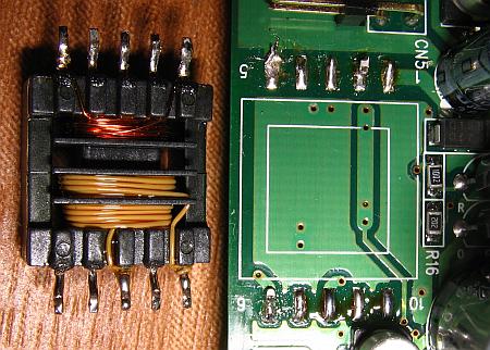
DC-DC converter filter chokes:
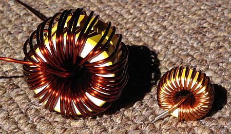 I ordered some T-184-26 cores, and
wound new inductors for the DC-DC converter's output filter. This photo
shows a new inductor side by side with an original one. The size
difference is pretty obvious, I would say! And even these much larger
inductors are still marginal, limited by the space available inside the
inverter. They have four times the inductance of the original
ones, and retain their inductance two times better at high DC current.
In addition, they loose only about 8 watts, instead of the 53 watts
lost by the original. 8 watts dissipation makes the big
inductor get warm, but not excessively hot, while the 53 watts
dissipated by the small one make it unsolder itself, loose
magnetic properties, discolor, or even self-destroy if run long enough.
I ordered some T-184-26 cores, and
wound new inductors for the DC-DC converter's output filter. This photo
shows a new inductor side by side with an original one. The size
difference is pretty obvious, I would say! And even these much larger
inductors are still marginal, limited by the space available inside the
inverter. They have four times the inductance of the original
ones, and retain their inductance two times better at high DC current.
In addition, they loose only about 8 watts, instead of the 53 watts
lost by the original. 8 watts dissipation makes the big
inductor get warm, but not excessively hot, while the 53 watts
dissipated by the small one make it unsolder itself, loose
magnetic properties, discolor, or even self-destroy if run long enough.
DC-DC converter loop compensation:
With the new filter inductor in place, at least I could test-run the
DC-DC converting section under stable conditions. So I ran it
in open-loop configuration, measured the real loop response, and
tailored an error amplifier to suit its phase/gain behavior. I finally
came up with a loop compensation that has 38dB gain up to 600Hz, then
starts falling off, introducing a total of three low-pass
poles, one of them dominant over the other two, to drop the
gain at high frequencies to a point that avoids too fast pulse width
changes, which could drive the push-pull converter into single-sided
saturation. All this while maintaining a very healthy phase
margin. With this error amplifier, the 340VDC output from this stage
stays regulated to within a few volts, even while the sine wave chopper
section draws a huge pulsed current, and remains fully stable under all
conditions tested so far. I don't know yet if this arrangement will
prove good enough in practical use, but at least there is hope...
More design mistakes showing up...
 While testing the complete inverter, suddenly
the output waveform started to degrade! While one half0cycle remained
clean, the other one distorted progressively, getting worse and
worse... After a while, it had become almost a triangle wave!
At the same time, the inverter started making quite horrible noises.
While testing the complete inverter, suddenly
the output waveform started to degrade! While one half0cycle remained
clean, the other one distorted progressively, getting worse and
worse... After a while, it had become almost a triangle wave!
At the same time, the inverter started making quite horrible noises.
The problem was quickly traced to one of the optocouplers in the sine
wave chopper not turning on correctly, producing erratic output. And
the reason for this problem, once again, turned out to be the utter
incompetence of the person who designed this circuit! A 6N137
optocoupler was being driven through a 1k resistor, from a 5V CMOS
driver output. This will produce about 3.6mA through the optocoupler's
emitter. And the 6N137 is rated for an absolute minimum of 6.3mA, with
a recommended value of 15mA! At 3.6mA, it will typically still function
at a low room temperature, but no longer when it gets even
slightly warm. As the optocoupler ages, it will progressively work
worse at that low current. How stupid is a designer who uses
1k resistors everywhere, without even checking the datasheets to make
sure the resulting current is in the safe range?
After swapping out those 1k resistors for a value that produces a
current in the safe range, the waveform returned to a good sine, and
remained there even when the inverter warmed up further.
Air flow:
A fan sucking air out of a closed box isn't much good, if air can't
enter the box! As described above, the air inlet openings on this
inverter's case total just 5% as much as the fan's active surface. To
gain some more air flow, I removed the two large power outlet
connectors. These multistandard connectors, that will mate with almost
any plug used anywhere in the world, worked well enough, but by
removing them and installing two standard Chilean outlets (the same
type as used in Italy), which are much smaller, I was able to free up a
lot of space on the front panel, which I gridded to use as air
inlet. The total opening area is now three times as large as before,
but that's still very small. I might need to drill a lot of holes into
the shells.
Grounding and bypassing:
 This inverter had a peculiar configuration: The
only part of it that was grounded in any way was the
enclosure. The entire circuit was left floating, including the battery.
The EMI filter at the output was also left ungrounded, and
thus useless. The battery was also floating. Worse than that: There was
a capacitor, installed by means of a piece of wire, joining the high
voltage DC bus to the low voltage (battery circuit)
side, which left the battery connected to 350 Volt pulses at 20
kilohertz repetition rate, respective to the AC output! This not only
turned the inverter into a highly effective broadband noise
transmitter, complete with dipole antenna (the high voltage wiring and
the battery wiring forming the two poles), but also made one get a
quite disturbing shock when touching the battery terminals!
This inverter had a peculiar configuration: The
only part of it that was grounded in any way was the
enclosure. The entire circuit was left floating, including the battery.
The EMI filter at the output was also left ungrounded, and
thus useless. The battery was also floating. Worse than that: There was
a capacitor, installed by means of a piece of wire, joining the high
voltage DC bus to the low voltage (battery circuit)
side, which left the battery connected to 350 Volt pulses at 20
kilohertz repetition rate, respective to the AC output! This not only
turned the inverter into a highly effective broadband noise
transmitter, complete with dipole antenna (the high voltage wiring and
the battery wiring forming the two poles), but also made one get a
quite disturbing shock when touching the battery terminals!
I had already reconfigured the output EMI filter to
actually work, by grounding its ground connection. Now I proceeded to
remove this stupid shock-generating capacitor, and then grounded the
negative side of the battery, which in fact means grounding
to the cabinet and thus to real earth the whole low voltage
and control circuit. This provides essential safety, and stopped the
shocks, but I quickly found out why the Power Jack people added this
capacitor: In the new, correct configuration, the control loop was
picking up a huge amount of that 20khz signal, driving the
loop wild!
 The
reason for this problem was quickly found: In his infinite wisdom and
experience, the person who designed the printed circuit board saw
nothing wrong in placing the feedback optocoupler over a "ground
plane". Nothing wrong with that, of course... except that the "ground"
he chose was the negative side of the DC link, which carries several
hundred volts of 20khz square wave respective to ground!
The
reason for this problem was quickly found: In his infinite wisdom and
experience, the person who designed the printed circuit board saw
nothing wrong in placing the feedback optocoupler over a "ground
plane". Nothing wrong with that, of course... except that the "ground"
he chose was the negative side of the DC link, which carries several
hundred volts of 20khz square wave respective to ground!
Look at the photo. The small white box is that optocoupler. On
the other side of the board there is a transformer. The
optocoupler base pin is directly over one of the secondary pins of the
transformer, which is at the high voltage side! There is a significant
capacitance through the board, directly coupling the several hundred
volts of noise into the highly sensitive optocoupler's base terminal,
which is not bypassed in any way!
Great design, don't you think? ;-)
To fix this, I lifted the optocoupler's base terminal from the board,
to reduce its capacitance to the noise "ground plane". Then I
put some bypassing on it, just enough to reduce the noise to an
acceptable level. And then I had to spent lots of time on doing some
magic tricks with the control loop, to make it stable again, because
the bypassing at the optocoupler inevitably degraded the phase margin
of the control loop to the point of making the circuit conditionally
unstable. At the end, it worked out well, but required international
help from two people who took an interest in this marvel of Taiwanese
engineering, and helped me with circuit simulations and suggestions!
Weak auxiliary power supply:
The little SMD transformer shown above is part of a galvanically
insulated auxiliary power supply that feeds part of the feedback loop,
and the drive of the sine wave chopper IGBTs. Such power supplies
should typically deliver about 15V. But this one only did around 11V.
With my new error amplifier, which took a little additional current
from this supply, the voltage dropped a little further. And
due to the unclever choice of filter capacitors and
high-side-driver bootstrap capacitors, strong current surges happen at
100Hz repetition rate. These surges ended up pulling the auxiliary
supply just below the 10V limit, making the bridge drivers drop out due
to undervoltage! The result was a horribly distorted sine wave
at the output.
 I first tried to fix the problem by
simply removing the transformer and adding a few
more turns to the secondary winding. When I removed it, I was
in for the next scare! This transformer has one winding doen with
common enameled wire, and the other winding uses wire with stronger
insulation. This is usual in such transformers that have to isolate
high voltages. But the person who designed this PCB negated
that safety by placing a groundplane under the transformer, that is
connected to the better insulated winding, and TOUCHES the
enamelled wire of the other side! Tehre are even some vias,
that don't have the green varnish on them, in contact with the
enamelled wire! So, in the original configuration of this inverter, the
only insulation between the 350V on the output side, and the battery
terminals, is a layer of wire enamel a few microns thick, which can
easily be scratched off!
I first tried to fix the problem by
simply removing the transformer and adding a few
more turns to the secondary winding. When I removed it, I was
in for the next scare! This transformer has one winding doen with
common enameled wire, and the other winding uses wire with stronger
insulation. This is usual in such transformers that have to isolate
high voltages. But the person who designed this PCB negated
that safety by placing a groundplane under the transformer, that is
connected to the better insulated winding, and TOUCHES the
enamelled wire of the other side! Tehre are even some vias,
that don't have the green varnish on them, in contact with the
enamelled wire! So, in the original configuration of this inverter, the
only insulation between the 350V on the output side, and the battery
terminals, is a layer of wire enamel a few microns thick, which can
easily be scratched off!
I added two layers of insulating tape before reinstalling the
transformer. Anyway, the insulation is still unsafe, because the tracks
on the PCB are too close together. On the right side of this photo, the
rectangular diode (in shadow) is on the secondary side, while the
groundplane around it is on the primary side. The clearance between the
two copper areas is far less than one millimeter.
At least I now have the battery circuit grounded, so that a
flashover at this place would cause damage, but no risk of
killing anybody.
Adding turns to the transformer only slightly improved the voltage.
Enough to stop the problem of the drivers dropping out, but just
barely. I later diagnosed the real problem as being a substandard PNP
SMD transistor that fails to meet its hfe rating, compounded by the
design using rather weak driving. I increased the driving, which
produced about 13V, which should be good enough.
At this point the inverter seemed to be working with an aceptable
performance. As a last improvement, I took out my wire clipper
and cut out two resistors that were causing totally
unnecessary power waste: One in parallel with the battery,
another one in parallel with the charger's AC input.
The one at the battery was probably intended to discharge the
filter capacitors after disconnecting the inverter from the
battery. It dissipated about a half watt at all times. This is not too
bad an idea, but I removed it because I want to be able to
leave the inverter connected to the battery at all times, even when
off, without draining the battery. The other resistor, at the AC input,
dissipated almost two watts and got very hot, and was totally useless.
I'm clueless as to why the designers included it. If it was to
discharge any tiny capacitances at the AC input after
disconnection, a megaohm resistor dissipating just milliwatts would
have been enough. There is such a megaohm resistor in the line filter I
added, so I could safely remove the 30k resistor that was causing heat
in an undesirable location, close to electrolytic capacitors
that don't like heat.
After that, I gleefully closed the cabinet! The inverter now works
reasonably well, doesn't cause too much interference, and should be
very much safer in every regard than it was before. Time will tell
whether it's now actually sturdy enough for practical use, or
if the poor heatsinking or some other uncorrected problem will kill it
again.
But I have the uneasy feeling of having been cheated. The engineering
effort I put into bringing this immature Taiwanese product to a point
at which it can be used, should have been made by the people producing
it, and not by me, the customer! My feelings of sympathy go to the many
people who bought one of these inverters, only to see it blow up, and
lack the expertise to correct its many flaws.
Back to homo ludens
electronicus.