Build a 13.8V, 40A Switching Power Supply
This compact and lightweight workhorse can power your whole station!
By Manfred Mornhinweg, XQ2FOD
This article was originally published (in a slightly modified form)
in the QST magazine, December 1998 and January 1999, and in the Radio Amateur's
Handbook, 1999. Visit the American Radio
Relay League for information on these publications, and a world of
ham radio related things!
Amateur radio has been somewhat slow to accept switching power supplies
for powering communication equipment. This is a pity, because "switchers",
as they are often called, offer very attractive features, like small size,
low weight, high efficiency, and low heating. True, they are generally
more complicated than linear power supplies, but this is easily compensated
by the fact that they can be built for a lower cost.
Some early switchers produced an objectionable amount of RF noise, bringing
the whole switching technology into bad reputation. But by proper design
techniques and careful EMI filtering it is possible to build very
quiet switchers.
In this article I will describe the construction of a switching power
supply designed to power a complete ham station, with several radios and
accessories. This power supply produces 13.8V regulated to better than
1%, at a continuous load current of up to 40A. It has current limiting,
making it appropriate for direct connection to a 12V backup battery. If
the current limit potentiometer is turned up, the power supply can deliver
up to 60A on an intermittent basis, while maintaining regulation. No minimum
load is required. The ripple on the output is about 20mV, and the efficiency
is 88%. A cooling fan operates depending on the average current drawn,
and a tricolor LED tells you if the voltage is normal, too high or too
low. It produces no detectable RF noise at any frequency higher than the
main switching frequency of 50kHz (I checked it with an antenna wire looped
around the operating power supply, tuning my TS450 from 30kHz to 40MHz).
And you get all this in a box that measures just 306 x 150 x 130mm, including
all projections, and weighs only 2.8kg!
Interested? Heat up your soldering iron and read on!
Linear versus switching supplies
You all know how a typical linear power supply operates: A heavy transformer
takes the line voltage and converts it into something slightly above the
desired final voltage. Some diodes rectify it, a big filter capacitor smoothes
out the DC, and a series pass transistor burns up the excess voltage, so
you get the desired output. A simple control circuit drives the pass transistor
to hold the output voltage constant. The circuit is simple and uses few
parts, but several of these parts are big, heavy, and expensive. And the
efficiency is usually only around 50%, often even lower. That produces
a lot of heat, which must be removed by big heat sinks and fans.
The switching approach is totally different: The line voltage is directly
rectified and filtered, resulting in about 300 or 150V DC (300 is more
commonly used). This feeds a power oscillator which produces output at
about 20 to 500 kHz. This relatively high frequency allows the use of a
small, lightweight and low cost transformer to reduce the voltage. The
output is then rectified and filtered. And now comes the most interesting
feature: Instead of just burning up the excess energy, in the switching
power supply the control circuit steers the power oscillator in such a
way that it delivers just the amount of energy needed. So, very little
energy is wasted, resulting in high efficiency (75 to 90%), almost no heating,
and a much reduced electricity bill!
Design decisions
There are several different topologies for switchers in common use, and
the first decision a designer must take is which of them to consider. Among
the factors affecting the decision are the power level, the number of outputs
needed, the range of input voltage to be accepted, the desired tradeoff
between complexity, quality and cost, and many more. For this power supply
I decided to use the half bridge forward converter design. This topology
connects the power transformer to a bridge formed by two power transistors
and two capacitors. It is reasonably simple, puts relatively low stress
on the power transistors, and makes efficient use of the transformer's
magnetic capabilities.
The second basic decision is which switching frequency to use. The present
trend is to use ever higher frequencies. But by doing so it becomes more
difficult to filter out the RF noise inevitably generated by the switching.
So I decided to stay at a low switching frequency of only 25 kHz for the
full cycle, which due to the frequency doubling effect of the rectifiers
results in 50 kHz on the output filter.
For the main switching elements, bipolar transistors or MOSFETs can
be used. Bipolars have lower conduction losses, while MOSFETs switch faster.
As in this design I wanted to keep the RF noise at an absolute minimum,
very fast switching was not desired, so I used bipolar transistors. But
these tend to become too slow if the driving is heavier than necessary.
So, if the transistors have to switch at varying current levels, the drive
to them must also be varied. This is called proportional driving, and is
used in this project.
The half bridge converter is best controlled by pulse width modulation.
There are several ICs available for this exact purpose. I chose the 3524,
which is very simple to use and easy to find. Any 3524 will do the job.
It can be an LM3524, SG3524, etc.
This basically ends the big decisions. From now on, designing the circuit
is a matter of calculating proper values for everything.
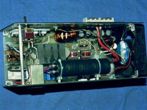
Circuit description
For the following explanation, refer to the schematic
diagram. Print it out, so you can follow the description on the drawing.
Line voltage enters through a CEE-22 connector with included fuse and
EMI filtering (P1). It is then passed through a 2-pole power switch, and
an additional common mode noise filter (C1, L1, C2). Two NTC resistors
limit the inrush current. A bridge rectifier delivers the power to a big
electrolytic capacitor (C3), which works at the 300VDC level. The power
oscillator is formed by Q1, Q2, the components near them, and the feedback
and control transformer (T3). T2 and the associated components act as a
primary current sensor. T1 is the power transformer, delivering about 20
V square wave to the Schottky rectifiers (D6..9). A toroidal inductor (L2)
and a six-pack of low equivalent series resistance electrolytic capacitors
form the main filter, while L3 and C23..24 are just there for additional
ripple reduction. The 13.8V is delivered to the output through a string
of ferrite beads with some small decoupling capacitors mounted directly
on the output terminals.
The control circuit is a 3524 IC (U1), powered from an auxiliary rectifier
(D17). The IC contains a voltage reference, oscillator, pulse width modulator,
error amplifier, current sense amplifier, flip-flop and driving circuitry.
It senses the output voltage and the current level, and through transistors
Q3 and Q4 controls the power oscillator. C37, C35 and R23 are used to implement
a full PID (proportional-integral-derivative) response in the control loop.
A quadruple operational amplifier (U2) is used for two auxiliary purposes:
To control the cooling fan according to the average current level, and
to drive the voltage indicating tricolor LED: It will glow green if the
voltage is OK, orange if the voltage is too low and red if it is too high.
How this thing works
When the unit is powered up, the first event that happens is a current
surge which charges C3. This surge is held at manageable levels by the
two NTCs, which offer about 2.5ê each when cold, and later loose
most of their resistance as they heat up.
As the operating voltage builds up on C3, R2 and R6 bias the two power
transistors Q1 and Q2 into their active zone. They start conducting a few
mA, but only for a very short time, because the positive feedback introduced
by T3 quickly throws the system out of balance. One of the transistors
receives an increased base current, coming from T3, while the other one
sees its base drive reduced. It takes just a fraction of a microsecond
to get one of the transistors saturated, and the other cut off. Which transistor
will start first is unpredictable, but for this analysis let's suppose
it is Q1. Notice that because the control circuit is not yet powered, Q3
and Q4 are off, so D12, D13 and D14 effectively isolate the 26-turn windings
of T3, the result being that they don't play any role for now.
T1 is now seeing about 150V across its primary. This produces about
+-20V on the secondary. The Schottky rectifiers rectify this, so L2 sees
20 V across it. This inductor will start taking an increasing current,
which is reflected back to the primary side of T1. The primary current
passes through the 1-turn winding of T3, forcing one-eight as much current
to flow into the base of the transistor which is conducting. This current
causes a voltage drop across R1 and R3, and this voltage is reflected back
onto T3. After some time the ferrite core of T3 will saturate, and this
will cause the base drive of Q1 to decrease sharply. Q1 will get out of
conduction, and Q2 will start conducting. Now the flux in T3's core decreases,
crosses zero, and increases in the other flow direction, until saturating
the core again, shutting Q2 off and Q1 on. Meanwhile the current in L2
builds up, and the filter capacitors are charged.
Notice that for safe startup it is necessary that T3 saturates completely
before T1 starts to do so. If this were not the case, the transistors would
have to switch under a very high and potentially destructive current. Keep
this in mind if for some reason you make changes to my design.
The power supply will oscillate freely for only a few cycles, because
D17 is already charging C32 and C33, powering up the control circuit. As
soon as this circuit gets enough voltage, it takes over the control of
the power oscillator. Let's see how U1 does this:
We will start at rest time, when both power transistors are off. U1
leaves both of its outputs (pins 12 and 13) in high impedance. So Q3 and
Q4 are biased into saturation by R15 and R16. Together with D13 and
D14 they place a dead short on T3's control winding. This keeps the voltage
across that transformer at zero, regardless of any currents that
may be flowing in the windings. C12 and C13, which are still charged from
previous conduction cycles, keep Q1 and Q2 biased to a negative voltage.
If now U1 decides that it is time to switch on Q1, it simply switches
pin 12 to ground. This switches off Q4, ending the short circuit on T3.
Through R14 and D12 about 15mA flow into the control winding center tap,
returning to ground via Q3. This puts about 50mA into the base of Q1, which
quickly switches on. Now the heavy collector current, which can be up to
8A at full load, adds up to the total current flowing in T3 and puts enough
drive into Q1 to keep it saturated at that heavy current. Note that by
this method the strong drive current for the power transistors comes from
the collector current via T3, so the control circuit does not have to provide
any substantial driving power!
If now U1 thinks that Q1 has been conducting long enough, it simply
switches off pin12. Q4 starts conducting again, shorting out T3. The current
in T3 is dumped into Q4, which may have to take up to 300mA. The
voltage on T3 breaks down, and Q1 switches off. Some time later U1 will
put pin 13 to ground, starting the conduction cycle for Q2.
U1 uses two input signals to decide what to do with its outputs. One
is a sample of the output voltage, taken through R25 and nearby components,
while the other is a current sample taken from the primary side by T2.
This is a current transformer that produces 200 times less current from
its secondary than what is put through its 1-turn primary. This current,
about 40mA at full load, is put into R12, producing a maximum voltage drop
of about 7V. This is rectified, the half of it is taken at the center tap,
divided down by R13 and VR1 and smoothed by C31. If VR1 is properly adjusted,
on the top of it you will get 200mV when the power supply is running at
full load.
The 3524 pulse width modulation controller is an interesting beast.
I suggest you take a manual of analog ICs from any of the manufacturers
that make this chip, and read through the 3524's data sheet. But I know
that you want me to explain how it works, so here I go:
An internal voltage reference puts 5V onto pin 16. R22 and R21 divide
this down to 2.5V, and apply this to the noninverting input of the error
amplifier. The inverting input gets the sample of the output voltage. With
13.8V on the output, and VR2 properly set, you are putting 2.5V into pin
1.
The error amplifier is a transconductance amplifier with 5Mê output
impedance. Its frequency and phase response, and its gain, are set by R23
and C35.
A second amplifier, specially included for current limiting purposes,
has its inputs at pins 4 and 5. This amplifier can be ground-referenced,
as done in this circuit, and has an internal offset of 200mV. That means
that it will pull down the main error amplifier's output if the difference
between pin 4 and pin 5 reaches 200 mV.
The chip contains an internal oscillator, whose frequency is set by
R24 and C36 to approximately 50kHz. The sawtooth output of this oscillator
is connected to an internal comparator, which has its other input internally
connected to the output of the error amplifier. The result of this is that
the output of the comparator will carry a square wave whose duty cycle
depends on the DC voltage at the output of the error amplifier.
Finally, an internal flip-flop distributes the resulting variable length
square pulses among the two outputs, which are uncommitted transistors.
In this design, the emitters of those transistors (pins 11 and 14) are
grounded, while the collectors drive Q3 and Q4.
During operation at medium to high load, the duty cycle is about 70%.
That means that at the cathodes of the Schottky rectifiers you will have
a square wave that stays at about 20V for some 14æs, and then slightly
below ground level for 6us. L2, which has its other end at nearly constant
13.8V, will therefore see about 6V for 14us, followed by -14V for the rest
of the time. Given its inductance of about 20uH, the current in L2 will
increase by about 4A during each conduction cycle, and decrease by that
same amount during rest time. As long as the current drawn from the power
supply is more than 2A, the current in L2 will never stop completely. For
example, if 20A are drawn, the current in L2 will vary between about 18
and 22A. As the ripple current stays basically constant while operating
at up to the maximum current of the power supply, the filter capacitors
C17 to C22 are never exposed to more than about 1.5A RMS total ripple current,
assuring them a very long lifetime. This is an advantage over some other
types of switching power supplies, in which the ripple current is much
higher, forcing the designer to use more expensive capacitors or to accept
reduced lifetime.
If the load is less than about 2A, the current flow in L2 is no longer
continuous. The duty cycle of the power transistors starts to drop, until
at zero load the duty cycle almost becomes zero too.
C37 serves several purposes. For higher frequencies it couples the first
filter stage (L2 and C17..22) to the error amplifier, while for lower frequencies
and DC the output of the supply is sampled. This is necessary because each
filter stage introduces 180 degrees of phase shift at the higher frequencies,
so after two stages the phase shift goes through a full 360 degrees, making
it impossible to stabilize the control loop without additional circuitry.
But for DC it is good to sample the output, in order to compensate for
the voltage drop in L3. So I chose this arrangement.
C37 was dimensioned to give the error amplifier a nice PID response,
together with R23 and C35. This affords the best possible transient behavior
and unconditional stability. In addition, C37 provides some measure of
soft starting, so the voltage does not overshoot too much when switching
on the power supply.
R34 and C38 average out the current level over a period of about 2 minutes.
U2C amplifies the resulting voltage by a settable amount, and U2D acts
as a Schmitt trigger to switch the fan cleanly on and off when the current
average crosses the trigger level set by VR3. R39 limits the speed of the
fan to a rather low value which is more than enough to keep the power supply
cool. At this low speed the fan produces almost no noise, and can be expected
to last longer than its owner..
U2A and U2B control the voltage indicator LED. They operate as follows:
An independent voltage reference (U3) delivers 5V to the noninverting inputs
of the opamps. If the power supply's output voltage is below 13.5V, both
pin 2 and pin 6 of U2 will be below 5V. So the outputs of these opamps
will both be high, lighting both the green and the red parts of the dual
LED. It will glow orange, indicating low voltage.
When the voltage is near 13.8V, pin 2 will still be below 5V, while
pin 6 will be above 5V. This switches the red LED side off, leaving the
LED glowing green, indicating correct voltage.
When the voltage rises to more than 14.1V, pin 2 will rise above 5V.
Pin 1 will go down, shutting off the green LED half, and pulling low pin
6 via D18. This will switch on the red LED side, so the tricolor LED now
glows red, giving overvoltage alarm.
If you use reasonably accurate resistors, this circuit needs no adjustment
to operate well.
Snubbering and EMI filtering
No transformer is perfect. Each winding has some inductance that is not
coupled to the others. And there is the magnetizing current, which in small
transformers can be a considerable part of the total current. At the end
of a conduction cycle, there is a strong current flowing in T1. After switching
the power transistors off, some means must be provided to discharge the
energy stored in the magnetic field of the core, and in the leakage inductances.
D3 and D5 were included for this purpose. They will recover most of this
energy and dump it into C3. Another portion will flow through the Schottky
diodes into L2, but this part cannot be more than whatever current is flowing
in L2 at the moment of switchoff.
A problem arises if the magnetizing current is bigger than the actual
load current, a situation that can happen especially during startup. Also
it must be taken into account that diodes, even fast ones, take some time
to switch, and the transformer cannot wait to start dumping its energy.
So some absorbing RC networks have to be included. They are commonly called
"snubbers".
R9 and C14 form the primary snubber, which absorbs energy during the
switching of D3, D5, Q1 and Q2. On the secondary side, R10, C15, R11 and
C16 protect the Schottky rectifiers against inductive spikes.
In this design I dimensioned these components in such a way that they
absorb considerably more energy than really necessary for protecting the
semiconductors. This causes some additional loss, but smoothes the switching
flanks, greatly reducing the RF energy generated. This is the first step
to make a ham-friendly switching power supply!
Of course, some RF noise is still generated. It must be cleaned up by
other methods. Some of them are obvious from the schematic, others
are not. The AC input is heavily filtered, first by the filter inside the
CEE-22 connector, which is effective against both common mode and differential
mode noise, and then by C1-L1-C2, which forms an additional common mode
filter. The two NTCs also add very slightly to the noise filtering. Between
C3 and the power oscillator two ferrite beads perform a critical noise
absorbing task. These are Amidon beads, made from 73-type material, which
unlike most ferrites has good absorption characteristics even in the lower
HF range.
On the output side, L2 already absorbs most of the noise. It is wound
on a high permeability iron powder toroid, which is very lossy in the HF
range. So it absorbs most of the HF energy reaching it. The main filter
capacitors are of the low equivalent series resistance type. This not only
reduces the ripple on the output, but also improves their usefulness as
noise filters.
L3 is another noise absorber. To minimize capacitive coupling over it,
I wound it on a ferrite solenoid instead of a toroid, so the input windings
are far apart from the output ones. The ferrite used is of the type that
starts absorbing at HF, so this coil like the others not only blocks, but
also absorbs RF energy. Finally, the output leads are passed through a
full dozen of 73-material ferrite beads. The filtering is completed by
proper bypassing of the output leads to the cabinet. It should be noted
here that the ground on the printed circuit board is floating, but the
enclosure is connected to earth. This arrangement reduces HF current flow
on the enclosure, which would lead the box to act as a noise radiator instead
of a shield! The power transistors and diodes are mounted in a special
way too, for the same reason. This will be described in the construction
section.
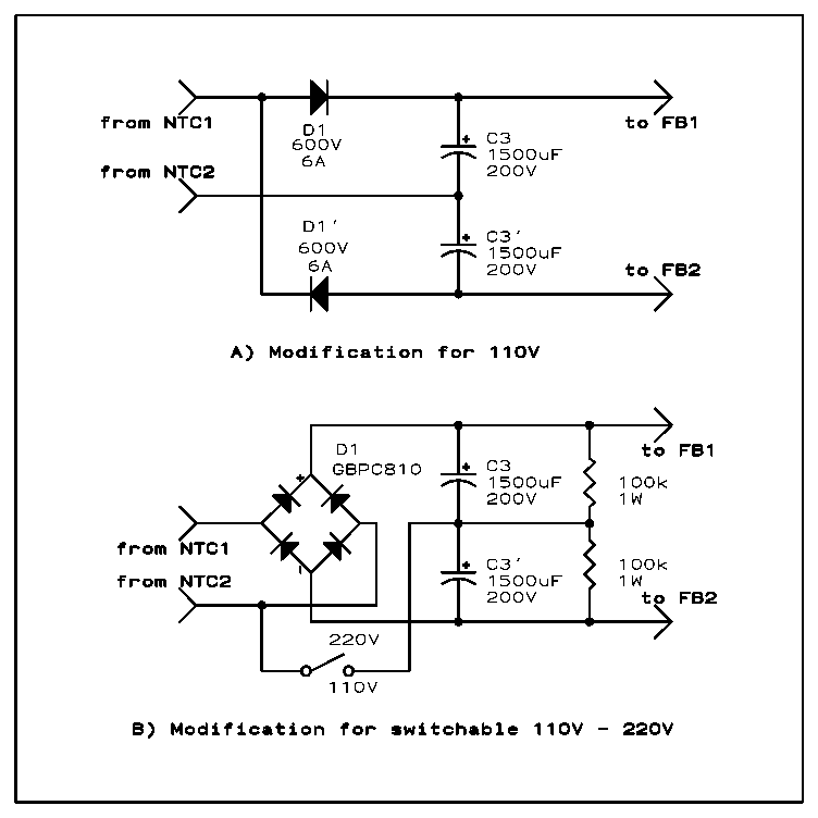
Running on 110V
I live in a country where the mains supply is 220V, 50Hz, so I designed
my power supply for this voltage. It will accept about 190 to 250V.
But switching power supplies are very easy to convert from 220V to 110V,
and it is even very easy to make them switchable between the two voltages.
This drawing shows how to do it. Basically,
you have to split C3 into two parts, connecting one side of the AC line
to the junction of the capacitors. This makes D1 work as a voltage doubler.
If you want only 110V operation, use the circuit in figure 2 A. As two
diodes of the bridge are not needed for 110V, they were eliminated, leaving
just two simple diodes.
If you want your power supply to be switchable between 220V and 110V,
you need to add a few more components. Part B of figure 2 shows how to
connect a switch to run the supply from either voltage. In this case, voltage-equalizing
resistors are needed across the capacitors, as shown in the diagram.
For 110V operation the fuse must be rated for 8 or 10A. The rest of
the components can stay the same, although you may replace the NTCs by
lower resistance ones, in order to maintain best efficiency. A pair of
1.3R NTCs should be about optimum for 110V. If you make the switchable
version, stay with the 2.5R NTCs, because they are needed for 220V operation.
If you choose one of these options, you will have to make the necessary
modifications to the parts list when you go shopping. But you will not
need to modify the printed circuit board other than drilling an additional
hole, because anyway C3 is not mounted on the board.
Finding the parts
You definitely cannot find all of the parts for this project at your local
TV spare parts store. You will have to order some of them by mail, unless
you live near a big industrial distributor willing to sell in small quantities.
But this is not too bad. Two mail orders plus some local shopping should
get you everything you need.
The biggest problem for most home builders is the magnetics. To keep
things simple, I used AMIDON cores, because this company accepts mail orders
for small quantities. The only exceptions are L1 and L3, which I took out
of my junk box. But both of these are uncritical, so nothing bad will happen
if you use parts that are quite different from
mine.
I found most of the other parts at local electronic suppliers. And I
live in Chile, where electronic parts are not too easy to come by. So anyone
living in more industrialized countries should have little trouble getting
these parts. But there are a few components which probably will have to
be ordered from a mayor distributor. Among these are the power transistors,
the Schottky rectifiers, the CEE-22 filtered and fused connector, the NTCs,
and the low ESR electrolytics. One very attractive supplier for these things
is RS Components, because this company sells almost everything in single
quantities, and has sales offices all over the world. Most of the difficult
parts for my power supply came from RS. The parts list gives RS Components'
part numbers for some items. I suggest you get a catalog from them. If
you want, you can order almost all the parts for this project from RS.
Other good suppliers include Farnell, Newark, Spoerle (in Germany) and
many more.
Here is a parts list. For some of the more
specific devices, RS stock numbers are given.
Please do not ask me to get the parts for you. I'm glad to give you
any advise and help needed to complete this project, but I do not provide
parts for it.
Winding the transformers and coils
 First things
first. Let's start with T1, the main power transformer, which can be considered
the heart of this circuit. I built T1 using a tape winding technique, and
stacking four pairs of ferrite E cores to get the necessary magnetic capabilities.
The manufacture of this transformer requires some handiwork, but it is
worth the effort. I will describe the process in detail, so you can exactly
follow the steps I took. If you prefer and have enough knowledge, of course
you can go your own route.
First things
first. Let's start with T1, the main power transformer, which can be considered
the heart of this circuit. I built T1 using a tape winding technique, and
stacking four pairs of ferrite E cores to get the necessary magnetic capabilities.
The manufacture of this transformer requires some handiwork, but it is
worth the effort. I will describe the process in detail, so you can exactly
follow the steps I took. If you prefer and have enough knowledge, of course
you can go your own route.
Because four cores are stacked, there is no factory-made bobbin available
for this transformer. So I made a paper bobbin. I wound the transformer
using copper strips interleaved with Mylar sheet, because the thick wire
necessary for the heavy current would be impossible to bend around the
sharp corners of the bobbin. Instead of using a lot of thin wires in parallel,
it is better to take this in a consequent manner and use copper tape. The
whole assembly was sealed in epoxy resin and the magnetic cores glued in
with epoxy. This is how you can do it:
First cut a piece of hardwood to serve as the winding core. As the center
legs of the four stacked cores measure 62 x 12mm, this wood block must
be 63mm wide and 12.5mm thick, to allow for some playroom. The length of
the block can be around 100mm, or whatever you prefer. The height of the
bobbin will be 28mm, so give theblock enough length to hold it with the
bobbin in place. If you have a low speed lathe, winding machine, or similar,
cut the wood block to such a length that you can mount it in the machine.
I used a belt sander to bring the wood block to the exact dimensions. Try
to be precise. If the block is too big, you will be wasting valuablewinding
space, running the risk of not being able to fit the windings. And if the
block comes out too small, your finished winding assembly may not fit the
ferrite cores, making it unusable.
Now wrap the wood block in one layer of plastic film, of the kind used
in the kitchen to preserve food. This material is an excellent demoulding
agent. Cut a strip of strong packing paper, 28mm wide and about 1m long.
Mix some 5-minute epoxy glue (I used the type sold in airplane modelling
shops, which comes in good sized bottles), and apply a layer of epoxy to
the paper strip. Now wind the strip very tightly around the plastic-wrapped
wood block, to make the bobbin core. It will be about 6 layers of paper.
Wrap another sheet of plastic film around your work, and press it between
two wooden blocks hold together with rubber bands, so the long sides of
the bobbin become flat and nice. Now get permission from your wife, mother,
or whoever reigns in the kitchen, and place the assembly in the oven for
about 15 minutes at 50øC. The epoxy sets much quicker and somewhat
stronger at that temperature.
Now you will need some copper sheet 0.1mm thick, and some Mylar sheet
of a similar thickness. Cut the copper in strips 22mm wide, and the Mylar
in strips 28mm wide. If you can make long strips, say 2m, this is an advantage,
otherwise you will have to solder individual copper strips together. In
total, you will need about 7m of copper tape and slightly less Mylar tape.
When you are ready with this, your epoxy has had ample time to harden,
so rescue your bobbin from the oven and go on. Take off the rubber bands,
the outer wood blocks, and the outer plastic wrapping (don't worry if it
doesn't come off completely). Do not remove the plastic wrapping that separates
the bobbin from the wood. You now have your wrapped wooden core and the
epoxy-paper bobbin on it.
Take a 60mm piece of #13 bare copper wire. Wrap the end of one
of your copper strips around the wire, so that the wire protrudes only
to one side from the copper sheet loop. Use a big soldering iron to flow
some solder into the junction. Try to avoid getting solder on the outside,
because this may later puncture through the Mylar insulation.
Now the winding starts. Position the copper wire on one narrow side
of the bobbin, so that the copper strip is centered on the width of the
bobbin, leaving 3mm room on each side. Stick the strip start to the bobbin
with some thin adhesive tape. Position the start of one piece of Mylar
strip so that it covers all the copper and is centered on the bobbin, and
tape it in place. Now wind 15 turns of this copper-Mylar sandwich, as tightly
as you can, keeping the Mylar aligned with the bobbin sides, and the copper
nicely centered. Don't loose your grip, or the whole thing will spring
apart. If your copper strip is not long enough, fix everything with rubber
bands or a clamp, and solder another copper strip to the end of the short
one, allowing 2mm of overlap. Before doing this, cut the first copper sheet
to a length such that the joint will be on one of the narrow sides of the
bobbin, because here you have space, while the wide sides will have to
fit inside the ferrite core's window. If the Mylar strip runs out,
just use adhesive tape to add another strip. Make the overlap 5mm, to avoid
risk of creepage between the sheets, and also try to locate the joint on
a narrow side of the bobbin.
When the 15 turns are complete, cut the copper strip to such a length
that the second terminal will be on the same narrow side of the bobbin
as the first terminal (the one you have already placed). Solder the second
terminal (another 60mm piece of bare copper wire) to the strip, position
it, and wind three or four layers of Mylar, to make a safe insulation between
the primary and secondary.
If you think this is a messy business, you are right. But it's fun too!
The secondary is just a little bit messier: It is wound with a five-layer
sandwich! Four layers of copper and the Mylar topping layer. But it's only
four turns total, so take a deep breath and do it!
First solder the four copper strips together around a piece of #13 copper
wire. Don't be overly worried if the outcome is not very clean; mine was
quite a mess too, and it worked well on the first try. Just be sure you
don't create sharp edges or pointed solder mounds, because these may damage
the insulation.
Now position the start of your secondary conductor in such a way that
the pin will come out to the same side as those of the primary, but on
the other narrow side of the coil assembly. So you will get a transformer
that has its primary leads on one extreme and the secondary on the other,
and will fit the printed circuit board nicely.
Wind two turns, solder the center tap wire between the four copper strips,
wind the other two turns, solder the last pin, wind a finishing layer
of Mylar and fix it in place with adhesive tape. Uff! This was the
worst part. If you reached this spot, you will have no problem building
the rest of this project!
What you have now is a springy, messy coil assembly that will fall apart
if you let it go. You have to seal it. This is easy to do:
Wrap your two wooden blocks, the same you used to press the bobbin,
in plastic film. Place them against the sides of the coil assembly, and
apply hard pressure, using a clamp or a lot of rubber bands, so that the
long sides of the coil straighten out completely, and any slack is displaced
to the narrow sides. Now mix a fair quantity of epoxy glue, place the coil
assembly so that the pins face up, and let the epoxy run into the coil.
Continue supplying epoxy until it starts to set. If it drips out from the
other side, no problem. Just don't do this work over your uncle's persian
rug. When the epoxy doesn't flow any longer, turn over the coil assembly,
mix a new batch of epoxy, and fill the other side completely, forming a
smooth surface. As the downside is now sealed, the epoxy will not flow
out there. And when this epoxy has set, turn the assembly over again, mix
epoxy, and apply it to form a smooth surface there. The idea is to replace
all the air between copper and Mylar sheets by epoxy, and specially to
fill the room left by the copper strip, which is narrower than the Mylar.
This filling is necessary both for mechanical and for electric safety reasons.
 Now convince
your kitchen's monarch that this devilish thing will add a nice scent to
the next apple pie, and place it in the oven again. Let the epoxy harden
completely, then remove the coil from the oven, remove the clamp, rubber
bands, wooden blocks, wooden core and all remains of plastic film..
And now comes the big WOW!!! You will be surprised how your messy
and springy assembly changed into a very robust, hard, strong and nice
coil!
Now convince
your kitchen's monarch that this devilish thing will add a nice scent to
the next apple pie, and place it in the oven again. Let the epoxy harden
completely, then remove the coil from the oven, remove the clamp, rubber
bands, wooden blocks, wooden core and all remains of plastic film..
And now comes the big WOW!!! You will be surprised how your messy
and springy assembly changed into a very robust, hard, strong and nice
coil!
Now test-fit the ferrite cores. See if they can be installed easily,
so that each pair of facing E cores gets in intimate contact without pressing
on the winding. If everything is right, the winding should have some playroom
in the assembled core. But it is easy to get too much epoxy on the coil.
If this happened to you, just take a file and work the epoxy down so that
it doesn't disturb the ferrite. The ferrite core MUST close properly, otherwise
you will later burn out the power transistors!
When the sizes fit, prepare some epoxy (again...!), apply a very thin
layer to all contact faces of the ferrite cores and mount them onto the
coil assembly. You can hold them in place with adhesive tape until the
epoxy sets. If you dare interrupting in the kitchen for a third time, use
the oven to quick up the hardening! The last thing you have to do
is bending the copper wires into the proper shape to fit the printed circuit
board holes. Be sure that on the secondary winding the center tap is actually
in the center position! The polarity of the other pins doesn't matter.
This completes
the manufacture of T1.
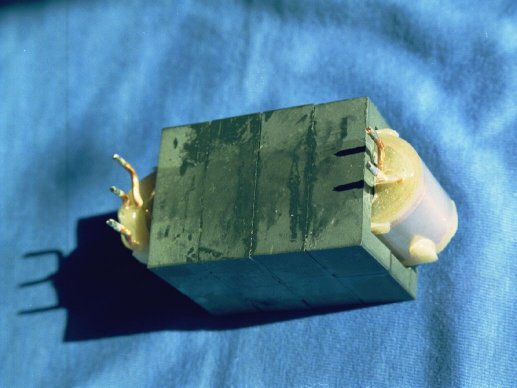
All the other transformers and coils are just child's play after making
T1. The current sense transformer T2 has a lot of turns, but there is absolutely
no need to wind them nicely side-by-side. You can use a winding machine
with turns counter, or you can just wind it by hand. Get some #36 or other
thin enameled wire, solder the end of it to one of the extreme pins of
the EE24-25-B bobbin, and wind 100 turns. Don't worry if your winding is
criss-cross and ugly, and don't feel guilty if you loose count and wind
a few turns more or less. As long as you don't overdo it, it will just
affect the position of VR1 when you align the completed power supply later.
Solder the wire tothe center pin of the same side, then wind another 100
turns in the same sense. Solder to the other extreme pin on the same bobbin
side, and apply one or two layers of Mylar, just to protect the thin wire.
Now take a piece of #15 plastic insulated cable, wind one single turn
over the Mylar and solder the two ends of the cable to the two extreme
pins of the other side of the bobbin. It doesn't matter which end goes
to which side. Install the EA77-250 core with a small amount of epoxy cement,
and T2 is ready.
T3 is made using the same type of bobbin and core as T2. First you wind
26 turns of #27 enameled wire. The 26 turns fit nicely in a single layer.
Wind a one layer of Mylar sheet, then put on the next 26 turns. Bring the
wires out to one side of the bobbin in such a way that they will not be
too close to the other windings. Wind 3 layers of Mylar tape, to give a
safe insulation between primary and secondary. Now, wind 8 turns of #20
wire, and solder the ends to the bobbin pins. Look at the printed circuit
board drawing to understand which wire to solder to which pin. Wind a single
layer of Mylar, then make the other 8-turn winding over the first one.
This will leave a space at one side of the bobbin which is big enough
to take the single turn of #15 plastic insulated cable, which completes
the assembly. Now glue the core in place with epoxy cement, and T3 is ready!
L2 is wound on an Amidon T-157-26 iron powder toroid core. As it is
too difficult to bend thick wire through a toroid, and tape winding it
is not practical either, I chose to make this coil with 10 pieces of #16
enameled wire in parallel. Cut the wires to about 1.5m length, and twist
them together. Then insert the bundle into the core, and starting from
the middle of the wire bundle, wind 7 turns, using half of the core's circumference.
Now wind the other 7 turns, starting from the middle towards the other
end of the wire bundle. The 15th turn is the one you made when you inserted
the wire bundle into the core! You will not be able to make a beautiful,
nice winding, as the total of 150 wires passing through the toroid is too
much to fit them in a single layer. But this doesn't matter at all, as
long as you get 15 loops of the wire bundle through the toroid's hole,
and there is plenty of space for this.
To make L3 you must first get a suitable core. I used a fraction of
an old ferrite antenna rod, which broke into several pieces when I let
it fall down... So, this is the recipe: Take an old ferrite antenna rod
of about 10mm diameter, throw it out of the window, go pick up the pieces
and select one that is about 50mm long! If you live in a 40th floor, better
don't use the window method. Instead, break the rod in some more
controlled way. You can't wind L3 on a bag of ferrite dust!
The winding itself is easy enough: Just wind 10 bifiliar turns of #11
enameled wire. This wire is quite stiff, but it is still no problem to
handle. I suggest you wind the coil on a 10mm drill bit, then spring it
open and place it on the ferrite core. Otherwise the ferrite could be cracked.
Fix the core in the winding with some epoxy. Bend the wires in such a way
that all four of them look down with the core straight up. That's the position
L3 is mounted on the PCB.
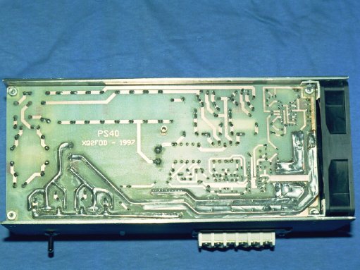
Making the printed circuit board
The exact size of the board is 120 x 272mm. It must be made from good quality
single-sided glass epoxy board. Pertinax material is unsuitable for two
reasons: The heavy components would stress it too much, and the copper
adhesion is not good enough for the heavy soldering required. This high
resolution GIF image provides the copper pattern
for this board, as seen from the components side. Note that many browsers cannot directly open this image due to lack of memory, as this is a 20 megapixel drawing. If you have this problem, right-click on the link, save it to your hard disk, then open it using a good image viewer or editor.
I suggest you make
a photographic reproduction of the design on Kodalith or similar high-contrast
film, adjusting it to the exact size. Then make the board using either
presensitized board material, or using untreated board and some POSITIV-20
or similar photoresist varnish.
You can of course make the board by some simpler method like ironing
on a photocopy, but I urge you to take the photographic approach. The better
quality is definitely worth it! I asked a professional photographer
and friend for help, and he took less than a hour to produce a professional
quality photographic mask from my original inkjet printout! Two hours later,
my board was ready.
Most of the holes are 0.8mm diameter. Others are 1mm, and a few are
bigger. My technique is first drilling everything with a 0.8mm dentist's
diamond drill, then measuring the pins of the bigger components and enlarging
the holes for them.
Assembling the board
This is probably the easiest step. Using the parts
placement guide, install and solder all of the parts except for Q1,
Q2, and D6..9. Before installing D1, you must fashion a simple heatsink
from a 30 x 80mm piece of 1mm thick aluminum sheet, bent into U shape.
Drill a hole into it and screw it onto the rectifier bridge, using a locking
washer. Then solder the D1 into the board.
All of the parts are mounted flush against the board, as it is not good
to have overly long leads. There are two cable jumpers on the board, drawn
as straight lines on the components placement diagram. The short one can
be made from a clipped component lead, while the longer one is made from
a piece of thin hookup cable.
Do not use IC sockets!!! These are an invention of the electronician's
devil! They introduce additional contact resistance, inductance and
capacitance, dramatically reduce the IC's cooling through the board, and
cause trouble later when the IC pins oxidize, or the chips simply start
falling out of the sockets. Don't tell me that you use good quality
sockets. They do exist, they are very expensive, but they cause much the
same problems. Keep in mind that modern ICs are made to be soldered! The
tinned pins can be soldered easily and safely, but even in gold-plated
sockets those tin-plated pins oxidize, insulating themselves. I'm
warning you so extensively because my job involves repairing electronic
equipment, and I can tell you that more than half of all problems are caused
by bad contacts, many of them in IC sockets!
Enclosure and final assembly
I have never liked using ready-made enclosures for my projects. It's easy
to make a custom box, and it will fit the electronics much better than
anything you can buy. This project was no exception, and so I made my own
box for it. But you are living in a free world, so do it however you want...!
I will not provide complete plans, but instead just outline my box design:
 Two 3mm
aluminum plates, measuring 300 x 120mm, are used as the front and rear
walls. They are screwed to the fan, the PCB, and to a 120mm long spreader
tube of 6mm diameter, so that these parts become integral to the structure.
The connections between the PCB, aluminum plates and fan are made with
small pieces of 10 x 10mm aluminum angle stock. The assembly is surprisingly
rigid!
Two 3mm
aluminum plates, measuring 300 x 120mm, are used as the front and rear
walls. They are screwed to the fan, the PCB, and to a 120mm long spreader
tube of 6mm diameter, so that these parts become integral to the structure.
The connections between the PCB, aluminum plates and fan are made with
small pieces of 10 x 10mm aluminum angle stock. The assembly is surprisingly
rigid!
The top and bottom covers are made from 1mm aluminum sheet and measure
126 x 300mm. The bottom cover has a hole for taking the center mount of
the PCB.The side covers are cut from wire mesh to allow unrestricted air
flow, and measure 122 x 126mm. The panels are held together by 10 x 10mm
aluminum angle stock, which runs along all edges, and by small sheet metal
screws. But these covers are not installed until the power supply is complete,
tested and adjusted. I painted all the panels flat black on the outside,
which looks nice together with the anodized aluminum angle stock. But I
kept the edges and insides free of paint, in order to get proper electrical
contact between the panels, and shielding action.
The components that are external to the PCB (P1, SW1, C3, the LED,
and the output screw block) are mounted to the front and rear panels. Q1
and Q2 are screwed to the rear panel, using M3 nylon screws and 3mm thick
ceramic insulators. These thick insulators were used not only for safety
reasons, but mainly because they reduce the capacitive coupling of the
transistors to the enclosure. This is very important, because if the unwanted
capacities at this place were significant, the switching spikes would be
coupled to the enclosure, causing RF current to flow on it and noise to
be radiated! It is of little use to filter the input and output leads,
if you make your shield radiate the noise by using too thin insulators
for the noise-generating transistors!
Do not use metal screws with plastic washers, because this approach
does not give enough safety margin to operate at line voltage. If you dislike
nylon screws, a good alternative are steel clamps that press onto the plastic
body of the transistors.
The Schottky diodes are mounted using the same kind of insulators and
screws, but there is a heat spreader, made from 6mm aluminum plate, between
those insulators and the case. All surfaces requiring thermal contact are
covered with heat transfer compound before assembly. When installing the
diodes and transistors, first do all the mechanical assembly, then solder
the pins. Otherwise you could stress them too much while fastening the
screws.
All cable connections are made next, and the output filter is assembled
by sliding the ferrite beads over the output cables and soldering the bypass
capacitors C25..30. Be sure to use a nice thick cable for the output!
40A continuous duty is no joke. I used a cable that has 4mm copper diameter,
plus plastic insulation. It was a surplus from the installation of an electric
winch in my 4WD vehicle. That cable is still a bit small for the winch,
but fine for this power supply!
 Now
you will need a big soldering iron (100 to 150 Watt) and a lot of solder.
The tracks on the secondary side cannot be trusted to carry the 40 or 60A
of this supply without some help! The necessary help comes in form
of some lengths of #13 bare copper wire. Cut and bend it to fit the shape
of all the high-current paths. Now take your big and very hot soldering
iron, and flow generous amounts of solder onto all of those tracks, so
that the reinforcing wire becomes buried in the solder. At the end, you
will have tracks in which the copper wire does most of the conduction,
while the solder couples the generated loss heat to the PCB, which dissipates
it. When you are ready with this task, your board will look terrible with
all that molten, burned and blackened flux residue! But don't despair:
Place the power supply in such a position that any liquid on the solder
side of the board can drip off, and now take a small paintbrush, a bottle
of alcohol, and applying generous amounts of this magic liquid brush all
of the ugly black rosin dirt away! You will be surprised at how easy
this is, and at how nice the board looks after this treatment! This photo
shows how mine looked after the alcohol bath.
Now
you will need a big soldering iron (100 to 150 Watt) and a lot of solder.
The tracks on the secondary side cannot be trusted to carry the 40 or 60A
of this supply without some help! The necessary help comes in form
of some lengths of #13 bare copper wire. Cut and bend it to fit the shape
of all the high-current paths. Now take your big and very hot soldering
iron, and flow generous amounts of solder onto all of those tracks, so
that the reinforcing wire becomes buried in the solder. At the end, you
will have tracks in which the copper wire does most of the conduction,
while the solder couples the generated loss heat to the PCB, which dissipates
it. When you are ready with this task, your board will look terrible with
all that molten, burned and blackened flux residue! But don't despair:
Place the power supply in such a position that any liquid on the solder
side of the board can drip off, and now take a small paintbrush, a bottle
of alcohol, and applying generous amounts of this magic liquid brush all
of the ugly black rosin dirt away! You will be surprised at how easy
this is, and at how nice the board looks after this treatment! This photo
shows how mine looked after the alcohol bath.
As the air flow from the fan will slightly shake the thin cables (those
connecting the LED, and the jumpers), it is a good idea to place some drops
of hot-melt glue at those places where these cables enter the board. This
will prevent fatigue and breakage of these cables. Hot-melt glue is also
an excellent material for fixing anything that would otherwise rattle,
like ferrite beads.
Testing and adjusting
At this time your power supply should be functional. If you have very big
self-confidence, or if you like surprises and enjoy fireworks, go ahead
and plug it in! But for everyone else, I would recommend this approach:
First, do a thorough visual check. Set the three potentiometers to mid
position. Check that there is no continuity between the AC input and ground,
between the AC input and the DC output, or between the DC output and chassis
ground.
Connect a variable voltage supply (you need 12 to 15V for the tests)
to the output leads, without plugging the switcher to the AC line. First
you should see the LED come up. Play with the voltage fed into your project
to see how the LED changes color. If this works, you will at least get
a confidence boost!
If you have a dual-channel oscilloscope, connect its two channels over
the base-emitter junctions of the power transistors. With the voltage at
about 12V, you should see small pulses with opposed phases. As you increase
the voltage, suddenly these pulses will disappear. If you want, you can
preadjust VR2 by setting your lab power supply to 13.8V and then setting
VR2 just to where the pulses disappear. Now it's time to start up the switcher.
Remove your lab supply, remove the oscilloscope leads, and connect the
beast to the AC line in series with a 60 Watt light bulb. This technique
will avoid most or all damage if something is wrong. Connect a voltmeter
to the output, switch on your baby and see what happens! If everything
is right, the bulb will light up, then slowly turn off, while the power
supply starts up and delivers about 13.8V.
Now, connect a load of about 2A to the output. A car bulb is very practical
for this. At this load level, probably the bulb in the AC line will glow,
while the voltage on the output may be 13.8V or somewhat below. It depends
on the specific current level drawn by your test load.
If so far everything is OK, the big moment comes: Remove the bulb from
the AC circuit! Now startup of the supply should be fast, and you can connect
a heavier load to it. With some load of 2 to 10A connected (the value is
uncritical, given the good regulation of this supply), adjust VR2 so that
you get exactly 13.8V at the output.
Next comes the current sensor adjustment. For this you need a load that
draws 40A! You can make it by connecting a lot of car bulbs in parallel,
or you can use some resistance wire to build a big power resistor. I made
a 13.8V, 550W heater to test this supply! Connect that load, and adjust
VR1 to such a position that the output voltage is just at the limit of
breaking down.
The last adjustment is that of the fan trigger. Connect a 65W car headlight
or similar load, which will consume about 5A. Leave it running for several
minutes, then move VR3 to the point where the fan switches on. Now check
out the trigger function by changing the load several times between about
2 and 10 A. The fan should switch off and on a half to one minute after
each load change. Eventually you may have to retouch VR3 until you get
the fan to switch on at no more than 7A continuous load, and switch off
at 4A or so.
The last test to do is to run the power supply at full load for a hour
or two. If it still doesn't burn up, you did a good job building it!!!
Complete the assembly of the enclosure, stick some self-adhesive rubber
pads to the downside, and you are R E A D Y !!!!!
And if it doesn't work?
If you are building this project, you probably already have some experience
in troubleshooting, so I don't need to teach you the basics. If you replaced
critical components like the power transistors, or the cores for T1, T3
or L2, this may cause problems. The power transistors MUST maintain their
beta up to at least 8A, otherwise they will cut short the conduction cycles
when the load increases. If you happen to replace those transistors by
some which have very low beta, the power supply may fail to start at all.
If you replaced the magnetic cores and did a bad choice, the results
can be quite dramatic. If T1 or L2 saturates, it can cause the power transistors
to explode before the fuse has a chance to open. The light bulb in the
AC line will avoid damage in this case, so by all means use that bulb for
first testing!
Another typical error is reversing the phase of some winding in T3.
If you get one of the 8-turn windings reversed, the results will be explosive
unless you have the light bulb in series. If you reversed the 1-turn winding,
the power supply will simply not start.
If you run into a problem which you can't solve, I will be glad to help.
You can contact me from the homo ludens homepage.
Back to the homo ludens electronicus
page.