Making printed circuit boards at home
using a laser engraver
 Printed
circuit boards are just one of many ways to build electronic circuits.
In the industry they are essential, because almost all of the automatic
production machinery is designed to use them. Instead for people
assembling circuits by hand, regardless of whether they are hobbyists
or professionals doing one-of-a-kind jobs, PCBs are entirely optional,
competing against other construction techniques such as dead-bug construction
on a ground plane, mounting parts into a box or chassis, using perfboards or project
boards, etc. Despite the various alternatives, many people choose PCB
construction due to the solidity, reliability, compactness, and sheer
good looks it provides.
Printed
circuit boards are just one of many ways to build electronic circuits.
In the industry they are essential, because almost all of the automatic
production machinery is designed to use them. Instead for people
assembling circuits by hand, regardless of whether they are hobbyists
or professionals doing one-of-a-kind jobs, PCBs are entirely optional,
competing against other construction techniques such as dead-bug construction
on a ground plane, mounting parts into a box or chassis, using perfboards or project
boards, etc. Despite the various alternatives, many people choose PCB
construction due to the solidity, reliability, compactness, and sheer
good looks it provides.
When I began building electronic
circuits, I soon also began making PCBs. At first I designed my boards
with a pencil on a piece of paper, then taped the paper to a piece of
copper-clad board, drilled the holes through the paper and the board,
then removed the paper and freehandedly drew the pads and traces on the
copper. I first tried to use a special felt pen made by Bishop
Graphics, which was supposed to be acid-resistant, but the results were
horrible! The ink of that pen did not fully block the ferric chloride
etchant I used, and the result were very poor PCBs, with seriously
corroded traces and many cuts. So I replaced that pen by a fine paintbrush
and oil paint. This paint was totally acid-proof, delivering shiny
copper traces, but it took at least a full day to dry, and the paintbrush in my
jittery hand produced traces of very unconsistent width. To fix the problem
of long drying time, I switched to fingernail polish, since various other paints I tried did not work
well. For several years I made all my PCBs using this method: Design
with pencil on paper, tape paper to board, drill the holes, remove the
paper, draw the pattern with nail polish, etch, remove the nail polish
with acetone, assemble the circuit. I even made double-sided boards that
way, by designing the board using two colors, and then simply painting
the patterns on both sides of a two-layer copper-clad board.
Over the years my designs became more
complex, and I needed a better resolution. So I began using photographic
transfer. I still designed the boards on paper, then placed a
transparent sheet on that paper, used dry-transfer rub-on symbols
made
by Letraset, Mecanorma and other companies to make the pads and
letters, then used black adhesive tape of various widths to make the
traces and areas. For double-sided boards, two such transparent masks were
made, and taped together. After very careful cleaning of my copper-clad
board, I sprayed it with Positiv-20 photoresist, made by Kontakt
Chemie, quick-dried it in an oven to reduce dust contamination, then
sandwiched the board and transparencies between two glass
plates,
and exposed the photoresist with near UV light. The light source was
always a bit of a problem: The high pressure mercury lamps recommended
in some literature didn't work at all, because they just don't produce
the wavelength required by this photoresist. Low pressure lamps worked,
but gave a diffuse light that tended to undercut the tapes and symbols,
resulting in narrowed traces. The sun at noon on a bright day in summer
was a pretty good UV source to expose PCBs, but usually when I made PCBs
the sky was overcast. At the end I settled for a 150W metal halide
lamp, which worked well enough, but I had to place it so close to the
board that the light fall-off in the corners was significant, causing
some problems of uneven exposure.
After exposure, the Positiv-20 photoresist was developed in a weak
solution of sodium hydroxide (lye). The instructions called for
precisely 7 grams per liter, but didn't mention that this was for pure,
anhydrous sodium hydroxide! Using that amount of the common household lye I could get,
which contains quite a bit of water, doesn't work well. By
experiment I found out that I had to use 10.5 grams per liter, and I
made a precision scale to measure the right amount. After depeveloping, the etching was done in
ferric chloride, just as before, and the photoresist was
removed
with acetone after etching. At this time I also became sophisticated
enough to spray a solder-through lacquer on my boards at this stage. It
used SK-10, also from Kontakt Chemie. Drilling the holes was
the
last stage in this process, and it was very easy and precise, with the
drill bit self-centering in the etched guide holes of
the pads. I
made many boards with this method, for projects such as various radio
transceivers, audio equipment, microcontroller circuits, test instruments, an EPROM
programmer, and many others. The resolution was good enough to pass one
track between pins of an IC.
In 1989 I started working for an
organization, got access to a PC, and with it began the age of CAD for
me. I left the paper and pencil behind, and began designing my PCBs on
the computer. I used several different programs at first, including
professional ones such as the very first release of OrCAD PCB (very
buggy!), Racal Redac (pretty good but user-unfriendly), and more basic
ones, such as smARTWORK, which I liked a lot and used a lot, despite
its somewhat limited capabilities - it could make only two trace
widths! Eventually I replaced them all by TRAX. All of these were DOS
programs, but by this time Windows was beginning to squeeze even into
engineering offices. At the job I eventually began using the
then-current version
of OrCAD for Windows, which was far less buggy than the first OrCAD PCB
for DOS, but also far more complex. The excessive complexity
became a real disease among all sorts of CAD software, so that for
my hobby
activities I began avoiding the big and famous software suites. For
PCBs I began using CiDess. After I retired from the job, becoming
a full-time homebrewer, CiDess became the only PCB design software I'm
using. It's pretty capable, and very suitable for homebrewers, even if
there are always some points that could be improved.
Back
in 1989 the only way I had to produce a high quality printout of a CAD
design was a pen plotter. We were several guys at the job occasionally
making PCBs, so many different combinations of pens and papers were
tried. It was always hard to produce a PCB mask by direct plotting,
that
would transfer well to the photoresist. What tended to work best was
using felt pens on translucent paper, and plotting the design twice to
get better opacity. The other option, of course, was to make a plain
black-ink-on-white-paper plot, take it to a photo lab, and make a high quality
positive transparency from it, using photolithographic material such as
Kodalith or
Agfa Litex, and special high-contrast developer. This also allowed
printing the design oversized, and photographically reducing it to the
exact size, which gave excellent resolution.
Eventually
I
implemented this same process at home. I had bought an HP inkjet
printer (black ink only) to replace my Epson dot matrix printer, and
the inkjet printer produced pretty good contrast, but not enough
resolution to directly print a PCB mask. I was given some expired but
still good Agfa
Litex material and special developer for it, and I put together a
sort-of-Frankenstein-enlarger.
The darkroom was my bathroom, with black cardboard used to seal the
window
against light,
and working in nighttime. Using this method I was able to produce very
high quality PCBs at home, but it took a huge lot of time and
effort for each board I made. Also the fact that I needed to print at
×2 scale to get a good resolution meant that I couldn't make PCBs
larger than half the linear dimensions of a legal-size sheet of paper,
the largest my printer could handle! Also I ran into barrel
distortion problems, caused by the enlarger lens. After some searching
and begging I got a better lens, which solved that problem, at
least.
There
came a time when photoresist spray became
unavailable in my country. And due to new postal regulations, things as
horribly dangerous as a spray can could no longer be shipped by mail,
so I
couldn't import that stuff either. I had to resort to presensitized
board, which is much more expensive, but is also more practical to use,
eliminating the cleaning, spraying and drying steps. I had mixed
experiences with pre-sensitized boards. I got some good ones, but also
some that had very low sensitivity, and some which had been handled in
strong
light, so that the margins (where light can get in under the black
protective film that covers them) had gone bad.
I also got
some boards that worked OK, but had extremely thin copper,
much
thinner than specified. You may guess where I got those from.
Eventually technology advanced, and I
bought a photo quality inkjet printer, that was capable of directly
printing good PCB masks on high quality transparency film (Pictorico
Ultra Premium). So I could get rid of my darkroom, and save several
hours of work when making a PCB. Unfortunately that printer (a Canon) was
extremely finicky, kept making trouble, wasting enormous amounts (by
cost) of ink in needless and seemingly endless cleaning cycles, and
ended its life three days after the warranty ran out,
producing an
error code that according to the information from the manufacturer
means that either the print head, or the mainboard, or the power supply
had gone bad, and that all three of them needed to be replaced at the
same time to fix the printer!
This was such an offense to logic and decency that I have sworn to never
again buy any Canon product.
So, once again I was on the
search for a good, practical process to make PCBs at home. Yes, I know,
well into the 21st century the way to go is to design my boards, create
Gerber files, send them to China, and get my boards factory-made in
professional quality. It's what most electronics builders do. But I kind of like
doing things myself, instead of having them done for me! Also there is
the problem that I live in the woods, quite literally, and there is no
delivery service that would come out here. So, getting anything from
China takes a long time, like several weeks in addition to the time
taken by the Chinese company to make my boards (which is actually
pretty fast), and them travelling to my country. So I wanted to
continue making my PCBs at home.
I
bought a cheap and merry laser printer, to replace the dead Canon
inkjet printer. It was a Brother, the cheapest one I could find. It
prints black only, of course, but does so pretty well, and hasn't given
any trouble at all since I bought it, several years ago. I like that!
In addition to
printing the usual stuff, like assorted love letters, shopping lists
and
schematic diagrams, I had hoped to be able to set up a system for
toner-transfer PCB making. But that never worked for me! I tried
several
different papers, including glossy magazine paper and special
toner-transfer paper, and I also tried different toners, and I tried
all
settings the printer has, which are not many - to no avail. The quality
of the PCBs I got
was horrible, with interrupted traces, corroded copper in any
filled areas, and there was
also
a dimension problem: This printer prints a little too narrow, but it's
not stable, every printout can be a little wider or narrower! In the
direction of paper transport it's quite accurate, but sideways it's
unstable. And the unpredictable part of the error is enough so that on
any but the smallest PCBs it's a problem. For its intended purpose,
printing documents, this slight dimensional inaccuracy is irrelevant,
of
course.
Eventually I
made up my mind that I needed some completely new device to get a PCB
design out of the computer and onto a copperclad board, and hopefully
one that would simplify the whole PCB making procedure to as few steps as possible. And
so I
finally decided to buy a laser engraver to make my PCBs. That was
successful, and the rest of this web page is, at last, about the matter
its title
says!
Making PCBs with a laser engraver
 For
those readers who don't know them yet: A laser engraver is a machine
that moves a powerful laser over a work area, under computer control,
modulating its intensity to selectively burn the material at the
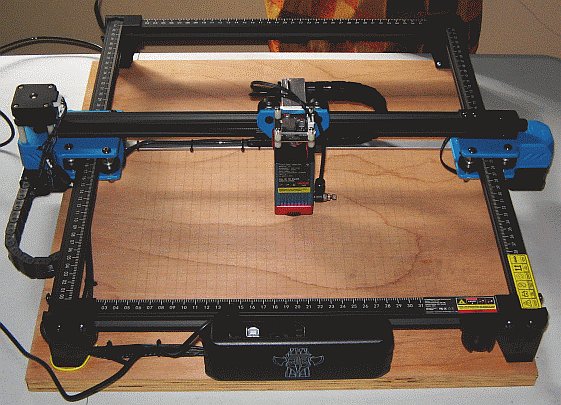
desired locations. The one I bought is a Two Trees TTS 55 Pro. It has a blue
diode laser rated at 5.5W optical power, with a lens that minimizes the
elongation of the laser spot. The machine has a working area of about
30×31cm, more than big enough for any PCB I will ever
make. Its
controller uses an ESP32 and runs pretty standard laser engraver
software, so it is compatible with the usual PC software, such as
LaserGRBL. The ESP32 has WiFi connectivity, and there is an SD
card slot, so the engraver can be used either connected by USB to a PC,
or connected over WiFi, or even stand-alone, engraving a board without
requiring any external control after starting. The file can be saved on
the SD card using a PC, or the card can be permanently left in the
engraver, and the files transferred by USB or by WiFi, from a PC or
even from a smartphone. Likewise, the unit can be controlled and
monitored from a PC or a smartphone, using either a dedicated app, or
a web browser, since the engraver provides a web interface. Also the
WiFi module can either connect to an existing WLAN, or it can act as
an access point. It's really very flexible and practical.
For
those readers who don't know them yet: A laser engraver is a machine
that moves a powerful laser over a work area, under computer control,
modulating its intensity to selectively burn the material at the
desired locations. The one I bought is a Two Trees TTS 55 Pro. It has a blue
diode laser rated at 5.5W optical power, with a lens that minimizes the
elongation of the laser spot. The machine has a working area of about
30×31cm, more than big enough for any PCB I will ever
make. Its
controller uses an ESP32 and runs pretty standard laser engraver
software, so it is compatible with the usual PC software, such as
LaserGRBL. The ESP32 has WiFi connectivity, and there is an SD
card slot, so the engraver can be used either connected by USB to a PC,
or connected over WiFi, or even stand-alone, engraving a board without
requiring any external control after starting. The file can be saved on
the SD card using a PC, or the card can be permanently left in the
engraver, and the files transferred by USB or by WiFi, from a PC or
even from a smartphone. Likewise, the unit can be controlled and
monitored from a PC or a smartphone, using either a dedicated app, or
a web browser, since the engraver provides a web interface. Also the
WiFi module can either connect to an existing WLAN, or it can act as
an access point. It's really very flexible and practical.
This
engraver comes prepared to add "air assist", which is simply blowing
fresh air onto the burn spot, to blow away any debris, and keep the
area from overheating. The required air pump is not included, so I
added one. But instead of buying the somewhat pricey pump offered by
the manufacturer of the engraver, I bought just a cheap aquarium airing
pump. Using this air assist is not essential, but seems to help a
little bit.
The manufacturer also offers a handheld controller. I did not buy that
one, since a smartphone can do its job well enough.
As
this engraver comes from the factory, it uses a rather ugly
method
to bring the wires to the moving parts: They are simply looped through
the air, inside flexible plastic slit tubes! They impose some
unstable load
on the mechanism, possibly reducing accuracy through flexing. So I bought one meter of
cable chain, and installed the cables in chain loops, so now they are
well guided. It looks much better, and is technically better too.
 Also
I screwed the engraver onto a piece of 20mm thick, very flat and
straight plywood, and then had the machine lightly engrave a
1×1cm grid over the entire work area. This allows easily positioning the PCBs
at known coordinates, and then commanding the machine to begin
engraving just at the right location.
Also
I screwed the engraver onto a piece of 20mm thick, very flat and
straight plywood, and then had the machine lightly engrave a
1×1cm grid over the entire work area. This allows easily positioning the PCBs
at known coordinates, and then commanding the machine to begin
engraving just at the right location.
There are many laser
engravers on the market, so if you want to set up for this method of
PCB making, you can choose the one you like best. But it's good to
compare specs, to select a suitable one.
Probably all of
the low-cost engravers use blue diode lasers. But there are differences
in the power, and the quality of the lens. Laser diode chips have a
rather long and narrow exit window, so they emit their light from a
surface of that shape. A common lens will deform and soften that image,
focusing it into a small but elongated ellipse of light. This is generally
undesirable, but many of the older/cheaper (as of 2025) laser units
have such lenses. Don't buy one of those, because those elliptical
spots are too long to provide acceptable resolution for PCBs!
The
better laser units instead have astigmatic lenses that produce a
rounder and more defined laser
spot. The advertising of my unit claims that the spot is a tiny square of 0.08×0.08mm,
but that's wishful thinking - it's still a bit elliptic! But it's small
enough to allow making even the finest PCBs, and that's what counts.
Another confusing matter is the power rating of these lasers. There are
three ways in use to rate the power:
- The optical power emitted (nominally 5.5W in mine)
- The electrical power consumed by the laser diode (roughly 15W in
mine)
- The electrical power required by an old-style carbon dioxide laser to
produce the same optical power (about 40W in mine)
So
when you compare specs, you absolutely need to know which "standard" is
being used to rate the power! Optical power is what counts. The more,
the better, but really high power lasers are an advantage only if the
modulation is fast enough to burn at a high speed and still get good
enough resolution.
When you go
shopping for a laser engraver, I suggest that you look at how stiff and
accurate the rails, wheels, and traction systems are. Mine uses plastic
wheels on extruded aluminium rails, and rubber belt drive. That works,
but is NOT ideal. Polished steel rails, with spring-loaded steel
wheels, and ball-bearing-screw-type drive, would be much better. And
also much more expensive, of course...
How the method works
The
basics are quite simple: The copper-clad board is coated with
black
paint, and allowed to dry. The PCB is designed in CAD, or
scanned from a
magazine, or whatever.
The goal is to end up with a precise raster image of the copper
pattern, in a file format like PNG, GIF, or BMP. Then a
converter program is used to turn this image into a long list of G-code
instructions, which the laser engraver can understand. The G-code file
is loaded into the engraver's SD card, or it can simply be
streamed to the engraver from a PC or smartphone. The painted (and well
dried!) board is placed in the engraver, the laser focus is
adjusted, the origin
(home point) is set, and then the engraver does its job. It will
burn
the paint in those areas where we need to remove copper. After
it's
finished, the burned paint residue needs to be cleaned away,
then the board is etched in
ferric
chloride or any other copper etchant. Then the remaining
paint is removed, optionally a solderable lacquer is applied, the holes
are drilled, and that's
it!
Since the devil lays in the details, let me now walk you through each
step.
Board material
It's a good idea to buy a reasonably large piece of board,
or several pieces, and clean and paint them all at once. They can be
stored for as long as wanted, and so there will always be a supply of
ready-to-use, painted, dry board at hand.
Copper-clad board comes in many types:
-
Base material: Most common and available are FR1 and FR4. Both are fire
retardant, but FR1 is basically paper impregnated in phenolic resin,
while FR4 is fiberglass impregnated in epoxy resin. FR1 is cheaper and
more gentle to the drill bits, while FR4 is stiffer, stronger, has
better copper adhesion, better insulation, and lower dielectric loss at RF. When I
was a poor student I used FR1, but since I began earning my own money I
only ever use FR4.
Other materials exist, and are common in
microwave work, high power electronics, and other special
areas,
but are not easily available to homebrewers in small quantities.
- Thickness: 1.4 to
1.6mm is by far the most common, and is a good all-round thickness. 1mm
is becoming somewhat common. Much thicker and much thinner boards
exist, but are rather hard to find.
- Number of copper layers:
You can choose between single-sided and double-sided board. If you are
like me, you will have good use for both of them, so it makes sense to
buy some of each.
- Copper thickness: The standard copper layer
thickness in the good old times was about 35µm, known in the USA as "1
oz copper", meaning one ounce of copper per square foot of board area. This
is a good thickness for typical PCBs. Instead for PCBs on which some traces
need to carry a high current density, 70µm copper thickness (2 oz copper) is better.
And board material intended for being used in processes that create
plated-through holes typically has only 18µm of copper thickness, or
even less, since this thickness will increase by galvanic deposition
when plating the holes. Such "1/2 oz copper" boards are not advisable
for use in processes that don't add more copper, but a
lot of such board material is currently available, simply because it's
cheaper than board having a normal copper thickness! So, be sure to
check that the board you are buying does have at least 35µm copper on
it, and don't buy from websites where you are likely to get cheated!
In
addition to all this, of course there are various qualities. Some boards
have a nice smooth finish, while other boards are quite irregular, with
the fiberglass fabric structure showing up through the copper.
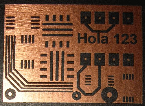
See the photo at the beginning of this page for an example of that!
Such roughness is not a functional problem, but a smooth board looks
nicer.
Some fiberglass boards are little fiber and much epoxy,
while others are the other way around. That makes a large difference in
stiffness, since glass is a lot harder than epoxy resin. Also the
dielectric constant and the losses vary between different boards.
Anyway the
good news is that all board material available will basically work. The most
important choices are between FR1 and FR4, and between single-sided and
double-sided board.
Before the board is painted, it should
be cleaned. Although the laser engraver PCB process is hugely more tolerant
of
dirt, grease and oxide than any photoresist-based one, a clean board
looks nicer and solders much more easily than a dirty one.
My
way of cleaning the board has two parts. The first is trying to not get
it dirty! Touching it with bare fingers will deposit skin acids on the
board, and the copper will start tarnishing in a matter of a few days.
Later one can admire one's fingerprints, nicely reproduced in black oxide on
copper background. Try to avoid that!
The second step is removing
light surface tarnishing by means of fine steel wool. Very
little pressure is used, or the copper will end up deeply
scratched. The game is all about wiping the surface in
both orientations, from all sides, not forgetting the borders and
corners, in quick moves at light pressure. That's all! Then all
steel wool debris and other loose dirt is blown or swiped away, and
it's done.
Paint
Now comes
the matter of paint. That's another big chapter! Much has been written
about what's the best paint for laser engraving. Enamel or lacquer,
what color, matte or glossy? Spray, or brushed, or spin-coated? I will
try to bring some sense into that.
First
let's
consider what paint is, really! What comes in a paint can is mostly a
mix of solvents. In some paints most of the solvent is water, while in
others there is no water at all. In the solvent mix is a smaller
amount of some synthetic resin -
think of it as a plastic, or plastic precursor, dissolved in those
solvents. Also there is a
tiny amount of finely divided pigment. Think of that as microscopic
dust grains of the desired color, possibly of several colors.
That's all
that
basic paint needs! But there are usually some additives. In high gloss
paints there are additives to
smoothen out the surface while drying, while matte paint contains a
significant amount of some coarser, inert material, such as talc or
silica. Think of it as very fine sand. Special paints, such as rust
protection or rust converter paint, contain specific chemicals for
those functions, and so on.
When the paint dries, the
solvent evaporates, and the resin polymerizes. What's left, in glossy
paint, is a clear plastic layer, in which there are zillions of little
colored particles. In the case of matte paint, the result is rather a
layer of fine "sand", with the colored particles lodged between
the sand grains, and some plastic acting as glue to hold it all
together.
Of course there are a lot more details regarding
paint, but this simplistic approach is all we need to select a good
paint for PCB making.
When the laser fires at the paint, the
plastic lets most of the light pass, but the little specks of pigment
absorb the intense laser light, and get very hot. What we need is that
these pigment particles burn the surrounding plastic, rather than getting burned
themselves! So that defines the two requirements for the pigment: It
needs to be of a color that efficiently absorbs blue light, and it
needs to be heat-resistant. Any color in the range of brown, red, orange,
yellow and green will absorb blue light well, as long as the color is
saturated. Black pigment will absorb all light, of course, including
blue. So what we need to avoid is blue paint, and anything containing
blue - which includes white, gray, and any unsaturated colors. That's
easy! But the heat resistance of the various pigments is
mostly
unknown to us. With one exception: Almost all black paint uses carbon
as the pigment, and carbon is highly heat resistant!
Bingo! Black
paint is fine, and since it's also widely available, and easy to see on
copper, we don't need to look any further. We use black!
The
next question is whether to use glossy or matte paint. Some people have
written on the web that it has to be matte paint, because glossy paint
reflects too much of the light. That's incorrect! In fact matte and
glossy paints reflect roughly the same fraction of the incoming light -
the difference is rather in how
they reflect it. While glossy paint reflects light in the same
orderly way a mirror does, with the exit angle being equal to the entry
angle,
matte paint scatters the reflected light in all directions. For PCB
engraving purposes, that's not a very significant difference.
 To
find out whether matte or glossy paint works better, I took a piece of board material and spray-painted one half
with glossy black acrylic paint, and the other half with matte black
acrylic paint. Both paints are of the same manufacturer and type. Then I burned a little test board design into each paint,
adjusting the parameters to get optimal results. What I found was
that matte paint is very forgiving: My first attempt turned
out
pretty good, and the second one was perfect. The glossy paint instead
was quite finicky, and I had to make 7 attempts before I found settings
that would produce perfect results. But then the resolution of the
glossy paint was better, and it doesn't need manual cleaning after
burning! Instead when using matte paint, most of the paint components
stay on the board after engraving, and need to be brushed and wiped off.
To
find out whether matte or glossy paint works better, I took a piece of board material and spray-painted one half
with glossy black acrylic paint, and the other half with matte black
acrylic paint. Both paints are of the same manufacturer and type. Then I burned a little test board design into each paint,
adjusting the parameters to get optimal results. What I found was
that matte paint is very forgiving: My first attempt turned
out
pretty good, and the second one was perfect. The glossy paint instead
was quite finicky, and I had to make 7 attempts before I found settings
that would produce perfect results. But then the resolution of the
glossy paint was better, and it doesn't need manual cleaning after
burning! Instead when using matte paint, most of the paint components
stay on the board after engraving, and need to be brushed and wiped off.
Where does this behavior come from? I think it's easy to explain,
considering the structure of each paint layer:
With
glossy paint, each little speck of carbon absorbs laser light, gets
hot, burns or evaporates the plastic around it, and as it's freed up,
it takes flight, going away with the stream of plastic vapor or smoke.
When only a very thin layer of paint is left, there are ever fewer
carbon specks remaining, so light absorption gets worse and worse,
hindering the burning of the last few microns of plastic that remain.
If I turn up the laser power like crazy, the paint around the laser
spot begins melting, and it flows out, re-covering the
surface already left behind by the laser! So it's hard to find the
exact right dose of laser energy.
The matte paint instead is
different: When a speck of carbon has burned all the plastic around it,
there is still the "sand" (talc or silica). This material is also
heat-resistant, and won't burn. So the carbon specks are trapped, and
can't take flight as easily as in the case of glossy paint. So they
keep absorbing energy from the laser, heating the remains of the paint
layer as long as the laser spot is
there, burning the plastic right down to the copper. The "sand" and the
carbon pigment remain in place, but are easy to clean away manually.
And
of course, the relatively coarse grain structure of the matte paint's "sand" causes
slightly worse resolution than with glossy paint, but it's still plenty
good enough. So my decision was: Matte black paint is best.
The
next decision: What resin should the paint be based on? Many resins are
used to make paints: Vinyl, acrylic, alkyd, polyurethane, polyester,
even cellulose acetate. I tried acrylic, alkyd, and cellulose-based
paints. Both blacks on my test board in the photo are acrylic paints, while
the red paint on the little scrap of board is cellulose-based. On the
back of that same board I tried flat black alkyd paint. They all seem
to work about the same, in terms of results, even if in the single test
I did with the cellulose paint the laser didn't burn through to the
copper, that red paint being glossy. But there are still some practical
differences: The alkyd paint smelled the worst during burning, and is
also the slowest-drying one, and more expensive than acrylic paint. For reasons of low
cost, quick drying, and low odor, I selected the acrylic paint as the
best option. I didn't try others, like polyurethane, because they are
supposed to be more heat-resistant, which is precisely what we don't
want!
Lastly: Spray paint, or brush the paint on, or use an
airbrush, or spin-coat the boards? For reasons of simplicity and
convenience, and given the wide tolerance the laser engraving process
has for uneven layer thickness, I settled for spray paint.
So my
recipe is: Use the cheapest available matte black spray paint available
in the local hardware store. And this is also the advice given by other
people who are using this method to make their PCBs, even if they
aren't as verbose as I am in explaining why! In my case the chosen paint
was
"Super Coat" acrylic enamel spray paint, made by Sherwin Williams in Brazil.
I
probably don't need to describe how to spray-paint a board... But just
in case: Place the board on a clean surface that you can make
dirty. Begin spraying outside the board area. Move over the
board
in lines, doing the reversing outside the board area. Spray until the
board is completely covered, totally black. Release the button outside the
board area. A good spraying distance is about 25cm. Since acrylic paint
dries fast, a longer distance can cause half-dry paint particles
to land on the board, making the layer rough and irregular.
Acrylic
paint dries in just about 15 minutes, but takes about a day to fully
harden (polymerize). Don't rush it. Store painted board material with
smooth separators between boards, to avoid scratching the paint. I
painted several pieces of single and double-sided board material I had
in stock, and stored them.
Board design:
As already mentioned, I currently use CiDess software to
design my PCBs. It handles single and double-sided boards, through-hole
and surface mounted parts, the SMDs can go on either side of a board,
it shows 3D previews, and it's quite usable after some practice. New
parts can be defined as required. Component placing and trace routing is all manual. A very important feature is that this
software prints guide holes in each pad, which is a big help at the
time of drilling. I would never use PCB software that can't
print guide holes!
CiDess always makes guide
holes proportional to the size of each pad. But I prefer having the
same small size of guide hole on all pads. That's easy to do, by
placing small pads on top of any large pads. The smaller guide hole of
the smaller pad will prevail.
One bad point is that CiDess can't make
arbitrary copper planes. Just a basic ground plane. It doesn't have a
fill function for arbitrary planes. So when an arbitrary copper plane is needed, I make a
trace that defines the contour, and then fill the area with wide
traces, to blacken it completely. Any guide holes in that black area
are still printed. That works fine, but is more work than just defining a contour and then pressing a fill button.
CiDess does not produce Gerber
files. It can
either print the layout directly on the local printer, which was very
useful to me when I printed masks for the photographic
process, or it can export the layout as BMP or GIF images, which is
what I use now. When exporting such a raster image, CiDess allows
selecting the scale in 13 steps, from ×1/4 to ×10. Each full
step
is 120 DPI, so the maximum scale of ×10 results in a raster image that
has the exact correct size when printed at 1200 DPI. To get the maximum
resolution and quality the program can deliver, I'm using 1200 DPI even
for boards that don't really need that much resolution, just for the joy of seeing a precise PCB!
Note
that the resolution to be used depends quite a bit on the laser spot
size of the engraver. If the spot is oval rather than circular, it also
depends on whether the laser scans along the long or the short axis of
that oval. Also it is possible to widen the spot by slightly defocusing
the laser, to burn wider lines and thus scan a large PCB in far less
time, but this requires a pretty powerful laser to still burn the paint
completely. So I suggest that if you want to try this method, with a
laser engraver roughly similar to mine, start out at a resolution
between about 600 and 1200 DPI, and go from there. 600 should be good enough
for through-hole PCBs, while SMD PCBs, specially for the 0.5mm pin
pitch ICs, will need 1200 DPI or better.
Whatever PCB software is used, it's necessary to end up with a two-color raster image of each
copper layer, where black is copper and white is no-copper, at a known
resolution, not mirrored (so that any text printed in copper is legible
in the image). General-purpose image editing software such as
IrfanView can be used to invert colors, invert or mirror images, crop the images, etc,
if necessary. With CiDess and my G-code converter, no such editing is required.
G-code conversion
Once
we have a raster image of the layout, it needs to be converted into
G-code, which is the language laser engravers understand. There are
several programs that will do this, both free and commercial ones. I
don't know about you, but I don't like paying for software! Instead I
prefer to use free software, and if none is available that does what I
need, write it myself and make it available for free. So I tried
the well-known and much-used LaserGRBL software, which in principle
does have all the features needed to take a raster image and
engrave it. The only problem is that LaserGRBL is aimed more at
artistic engraving, such as burning a photo of a landscape onto
a piece of wood. When trying to burn a
high-resolution PCB, LaserGRBL quickly
hits its limits, particularly in combination with inexpensive engravers
that have a lot of backlash, elasticity and friction in their moving
parts. The quality I got was unacceptable.
There are two
fundamentally different ways to burn such an image. One is to move the
laser to the beginning of an area that needs to be burned, turn it on,
and then move it smoothly around in that area, like a farmer mowing a
field, making turns, lines, whatever, to cover the entire area in the
least possible time, without passing twice over the same spot. Then
turn off the laser, move to the next area to be burned, and begin
burning there. This method requires moving the laser in all directions
while
burning, and that will only be accurate if all the structures, rails,
wheels, motors, belts, etc, are stiff and precise enough, and if the
motions are slow enough so that inertia and flexing are irrelevant. In
low cost
laser engravers the mechanisms are stiff and precise enough to engrave
a picture
that will be viewed from one meter distance, but they are neither stiff
nor
precise enough to engrave a PCB in that way, particularly not one
intended for SMDs.
So
we need to resort to the other method: The laser scans the image area
in lines, covering the whole width of the PCB plus some margins for acceleration
and deceleration. The laser is pulsed on and off to burn the
paint where it should, and leave it intact where we want to end up with
copper. Burning is done only while moving in one direction. During retrace the laser
is always off. This is very much like the sweep of a CRT TV or monitor. With
this method, backlash doesn't matter at all, and lack of stiffness
matters very little, because the laser head accelerates outside the PCB
area, stabilizes its motion, and then just moves smoothly at constant velocity while engraving.
But
LaserGRBL doesn't have this mode! It can indeed do scan lines, but it
cannot accelerate outside the image area. Some commercial programs have
that mode, but I like free software...
So I wrote my own program
to do the G-code conversion. It's just a very basic (literally, written
in BASIC language!) command-line program, but does the job quite well.
It directly reads the raster files exported by CiDess, or any other PCB
software that can do that, from the PCB program's directory, handles
all the conversion, and leaves the G-code file in the directory defined
by the user. A configuration text file allows setting the source and
destination directories, DPI, laser power, burning speed, overscan
width (for acceleration), and it also allows setting correction
parameters to compensate for the effective size of the laser spot.
These parameters are separate for X and Y, so that the dimensions of an
elliptic laser spot can be correctly compensated for.
If you
want to make PCBs with a laser engraver, and you want to use my
program, you are welcome. Just download it, unzip it into a directory
of your choice, edit the .cfg file to reflect your needs and
preferences, and send the .bat file to the desktop or into your start
menu. To use the program, you click that icon, enter the filename of
your PCB raster file, and the program will do the conversion and give
you a report.
Raster image to G-code
converter
The
configuration parameters in the provided .cfg file are the ones I
currently use. Most likely you will need to modify some of them. The file
includes some hints and instructions.
If you have the bad idea
to feed a color or grayscale image into this converter, or if you use a
lossy-compressed file format like JPG, the program should try to sort
all colors or gray levels so that the darker half is considered copper,
and the lighter half no-copper. I don't know how well that would work,
since part of the functionality is in an external library my program
uses. Better avoid it, and use only lossless black/white image formats.
Laser engraver setup
 Laser
engravers support a set of configuration commands. LaserGRBL and
similar programs can be used to access the machine's configuration, and
change the parameters as needed. Most parameters are
properly
set at the factory, but there is one that absolutely needs to be
changed, to make good PCBs! That's the laser PWM frequency, parameter
$28. The factory setting is 1000Hz. At that low frequency, and any
power setting below maximum, the laser pulses slow enough to results in jagged
traces! See this photo of a small test PCB, and pay attention to the
vertical lines, particularly the ones at the very left. You will see
some of them having zigzag borders. This is an interference pattern
between the laser head motion frequency and the laser's PWM frequency.
Laser
engravers support a set of configuration commands. LaserGRBL and
similar programs can be used to access the machine's configuration, and
change the parameters as needed. Most parameters are
properly
set at the factory, but there is one that absolutely needs to be
changed, to make good PCBs! That's the laser PWM frequency, parameter
$28. The factory setting is 1000Hz. At that low frequency, and any
power setting below maximum, the laser pulses slow enough to results in jagged
traces! See this photo of a small test PCB, and pay attention to the
vertical lines, particularly the ones at the very left. You will see
some of them having zigzag borders. This is an interference pattern
between the laser head motion frequency and the laser's PWM frequency.
Increasing the PWM frequency to 10000Hz solves this problem.
Some
other parameters might be of interest. Parameter $50 sets the WiFi
mode, with 0 being off, 1 making the machine act as an access point,
and 2 making it try to connect to an existing WLAN. When operating as
access point, parameter $51 sets the network name, and $52 sets the
password. Instead when connecting to an existing WLAN, parameters $53
and $54
set the network name and password.
Parameter $100 sets the steps per millimeter for X, and parameter $101 sets it
for Y. These come factory-set to the nominal values for the machine, which are
precise as long as the belts of the machine have exactly the correct
tooth pitch. If the belts are too tense, or too loose, they stretch or
contract a little, and that makes the dimensions of the engraved PCBs slightly
imprecise. So an important part of the initial setup is to check the
precision of X and Y dimensions, and if it's not good enough, either
tensing or loosening the relevant belt a little, or adjusting these
configuration parameters. They accept decimals, even if the nominal values are usually integers.
All the other parameters are usually fine as they come from the factory.
After
changing any parameters, there is a command that has to be given to
save the changed parameters into non-volatile memory. After that, the
parameters will stay, and don't need to be checked for every PCB.
I
also made a hardware adjustment: The X motor of my engraver ran
extremely hot. The operating currents for each motor are adjustable by
means of tiny potentiometers inside the controller. I reduced the
setting until the X drive began losing steps when accelerating, and
then increased it to a middle point between that limit and the original
position. At that setting the motor runs cool, and no steps are lost.
Engraving
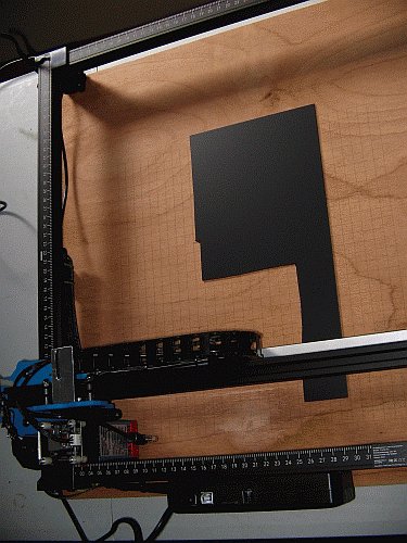 This
is my workflow to engrave a board: First I set up the engraver on a
desk in my guest room, because in my office/workshop/radio room I simply never have
enough free desk surface. The guest room is usually unoccupied, due to a severe and chronic lack
of guests. Accessing the engraver's web interface over WiFi through my
LAN from my PC, I upload the G-code file created by my converter
program.
This
is my workflow to engrave a board: First I set up the engraver on a
desk in my guest room, because in my office/workshop/radio room I simply never have
enough free desk surface. The guest room is usually unoccupied, due to a severe and chronic lack
of guests. Accessing the engraver's web interface over WiFi through my
LAN from my PC, I upload the G-code file created by my converter
program.
Then I place the painted board on the work surface,
check/correct the laser focus with the tool that comes with the
engraver, and then carefully align
the board to the grid. It can be placed anywhere in the workspace, and
it's a good idea to place each board at a somewhat different location,
in order to wear the rails and belts more evenly. To keep the laser
from burning the wooden base, and to allow precise finishing of the
PCB's borders, I place my board so that the lower left corner of my PCB
will be about 2mm inside of the raw board's edges. With single-sided
boards, alignment isn't critical, the only goals are that the whole
design fits on the board, and not too much board area is wasted. With
double-sided boards instead, precise alignment is needed, which can be
done by cutting the board to a precise size, including a small but
precisely known margin, and aligning it very well to the grid each
time. It's also possible to drill two holes through the board,
symmetrically and outside the PCB area, and drill them all the way into
the wooden base, or into another piece of wood that is then placed on
the work area. Then the board can be pinned down, the first side
engraved, then it's flipped over and pinned down in the exact same
location, and the other side is engraved.
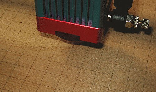
The
grid I engraved on my plywood base has its origin 1mm up and right
from the left lower corner. Since this engraver has no init switches
nor sensors, I turn off the engraver and manually push the laser head
fully into the left low corner, where it is shown in this photo, and
then I switch the engraver on. Then I access the engraver from my
smartphone over WiFi, and use the commands provided to move
the
head 1mm up and right. Now I have it at the origin of my grid. Then I
use the commands to move the head to the lower left position of my PCB,
as counted on the grid lines. I visually
check that now the laser head is centered in X and Y on the grid lines
where I want my PCB to begin, to rule out any gross mistakes.
The G-code
my converter program produces assumes that the left low corner of the
total
scan area, including the overscan, is the home (reference)
position. So
I need to move the laser head left, by just as much as the width of my
overscan area, defined in the configuration file of my converter. Since
I use 5mm, I move the head 5mm left, by the interface
commands. Now the head is exactly at the beginning of the desired scan
area, and I set the new home position there, by the interface
command. To check that it is correct, I move the head away
a random amount, by interface commands, then command it to
return
to home, and visually check that it returned correctly. After that I
command the machine to begin engraving the G-code file of my new PCB,
stored on its SD card. Then I can walk away and let the machine work. I
can check the progress on the smartphone. A modern world this is...
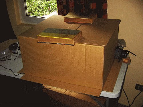 Even
if acrylic paint proved to be the least smelly while burning, it's
definitely not odor-free. At first I simply opened the window and
closed the door of my guest room, but the smell tends to cling to the
room, and is detectable even the next day. So I crafted this fancy
smoke hood from an old cardboard box and some hot-melt glue. I turned the
box inside out, so that all the advertising for its original contents
isn't visible. It looks far more decent that way!
Even
if acrylic paint proved to be the least smelly while burning, it's
definitely not odor-free. At first I simply opened the window and
closed the door of my guest room, but the smell tends to cling to the
room, and is detectable even the next day. So I crafted this fancy
smoke hood from an old cardboard box and some hot-melt glue. I turned the
box inside out, so that all the advertising for its original contents
isn't visible. It looks far more decent that way!
The top
cover is easily lifted off, to access the engraver. To keep it in place and reasonably well
sealed, I use some honorable, ancient and heavy literature. This
is vivid proof for the fact that books are still useful, even
in
the age of the Internet!
There is an exhaust fan installed on
the box, visible on the right side. A lightweight and flexible hose
connects to it, and sends the smoke out of the slightly ajar window.
Air
enters the box only through the imperfect seals between the
box, the
cover, and the desk. This creates an extremely small
underpressure in the box, which is enough to completely prevent
any smell from escaping it.
The
engraving process is slow. I need to stress that point! This
PCB production method is unsuitable for producing large amounts of PCBs, due to its
slowness. But it's perfectly suitable for homebrewers who just make one
occasional board every now and then. While the engraving process is
slow, it's totally automatic, and requires no attention, except that
somebody should always be around and ready to act in case anything goes
wrong. Should the machine fail, the laser could conceivably end up
turned on and pointing at a fixed spot of the wooden base, possibly
setting it on fire! Since I'm just one room away while the engraver is
working, that's not a problem for me, but if anybody needs to let such
an engraver work completely unattended, for example overnight when
everybody sleeps, it might be a good idea to use a metal base instead
of a wooden one, so that nothing can catch fire, even if a
malfunction happens.
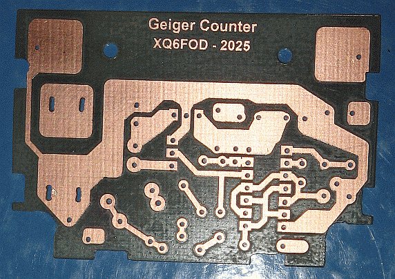
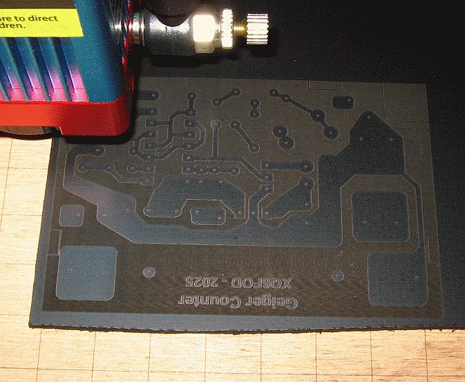
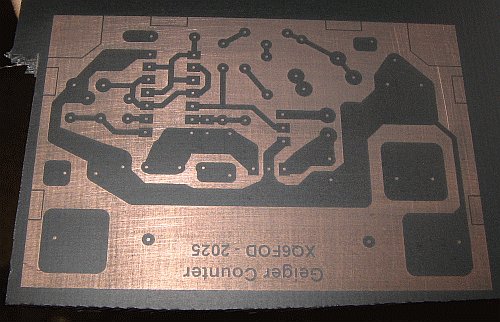
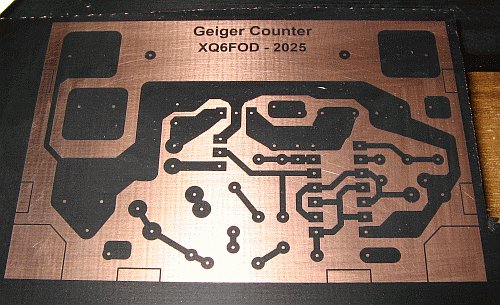
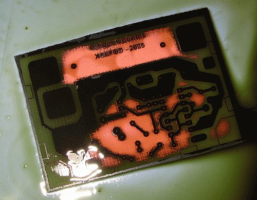
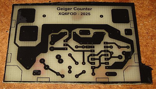
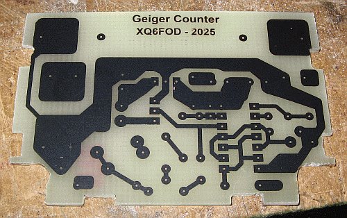
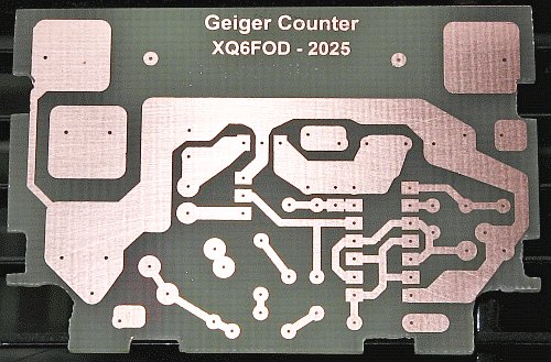
The Geiger counter PCB shown in this page
measures 73×50mm, and took roughly 50 minutes to engrave.
Since
the time needed is roughly proportional to the PCB area, an Eurocard
might take slightly less than three and a half hours, and a
really
large board might well take a full day. I have my system configured to
engrave at a speed of 6000 millimeters per minute (that's the unit used
by this engraver). So, to scan the 73mm width of the board, plus the
10mm total overscan, 0.83 seconds are needed per line, plus some small
time for acceleration. The retrace is faster than that, and happens at
the acceleration and maximum speed configured by the
manufacturer of the machine. These are an acceleration of
2500mm/s², and a speed of 30000mm/min, again using the units set by the
manufacturer of the machine. All this results in a total time of
slightly over one second per complete line, including the retrace. Since I
engrave the boards at 1200 DPI, that's roughly 0.021mm per line. With
this board measuring 50mm in the Y dimension, it requires about 2362 scan
lines. At a little over 1 second each, there we have the roughly 50 minutes
it took.
Due to the time used to scan the overscan area at the
sides of the PCB, and the acceleration and deceleration, it's faster to
engrave a given board with its long axis in the X orientation, rather
than in Y. So any board that was designed with its long axis in Y
should be rotated by 90°, to make the engraving process as fast as
possible for the parameters used.
Out of fear of shortening the
life of my laser diode, I set the laser power to 75% of the maximum.
This might not be necessary, considering that anyway the laser is off
during retrace, also over the overscan areas, and of course when moving
over any areas where the copper is to be preserved. To get maximum
engraving speed it would be wise to set the laser to 100%, and try what
is the maximum speed at which the paint is still burned well
enough. Also the resulting accuracy needs to be watched, because at a
higher speed there will be more imprecision coming from the timing
accuracy limit of the laser on/off control.
At the current stage of my
life, electronics is a hobby for me, not a job anymore, and so I just
let the machine take the time it needs to do the job well.
Cleaning the paint residue
 This
is how the board looks when engraving has finished. All of the paint
still seems to be there, and it just looks roughened in the areas where
the laser burned it. But make no mistake! The laser thoroughly
destroyed the paint at the places it hit. The talc powder and the
carbon pigment particles are still there, but only very loosely bound
to each other and the board, by charred residues of the resin.
This
photo also shows quite well how the lower left corner of the PCB ended
up exactly where I wanted it, at a crossing of two grid lines, leaving
an adequate margin on the raw board. You can see better than in other photos how I aligned the board to the grid.
 This
is how the board looked after brushing off the loose paint residue with
a paintbrush. A soft toothbrush can also be used, with care to not
damage very narrow traces.
This
is how the board looked after brushing off the loose paint residue with
a paintbrush. A soft toothbrush can also be used, with care to not
damage very narrow traces.
Some paint residue sticks to the copper a little more firmly, and needs
to be removed in a second cleaning step.
 The
second cleaning step is wiping the board with a piece of paper towel
soaked in alcohol. I tried both ethyl and isopropyl alcohol,
and
both seem to work well. Water instead did not work well, showing that
some slight solvent action is required. I suspect that the laser's heat
thoroughly depolymerizes the acrylic binder, so that what's left is
soluble in alcohol, while the non-lasered paint remains polymerized and
insoluble in alcohol.
The
second cleaning step is wiping the board with a piece of paper towel
soaked in alcohol. I tried both ethyl and isopropyl alcohol,
and
both seem to work well. Water instead did not work well, showing that
some slight solvent action is required. I suspect that the laser's heat
thoroughly depolymerizes the acrylic binder, so that what's left is
soluble in alcohol, while the non-lasered paint remains polymerized and
insoluble in alcohol.
To make sure that no thin film of paint
remains on the copper that will be etched away, a good test is to take
a multimeter that has a good, instant-reacting continuity beep
function, connect one test lead firmly to the copper, and very lightly slide
the other test lead over the copper surface, in several areas. It
should produce a continuous beep. If the beep is
intermittent, probably more cleaning with alcohol is needed,
or
the board wasn't lasered well enough.
 I
cut my PCB from the raw board only after confirming that it's good and
ready for etching. In case the lasering went wrong, I would simply try
again in another corner of the raw board, with corrected settings, and
later on remove the paint from the rest of the board, and repaint it.
That way no board material goes to waste.
I
cut my PCB from the raw board only after confirming that it's good and
ready for etching. In case the lasering went wrong, I would simply try
again in another corner of the raw board, with corrected settings, and
later on remove the paint from the rest of the board, and repaint it.
That way no board material goes to waste.
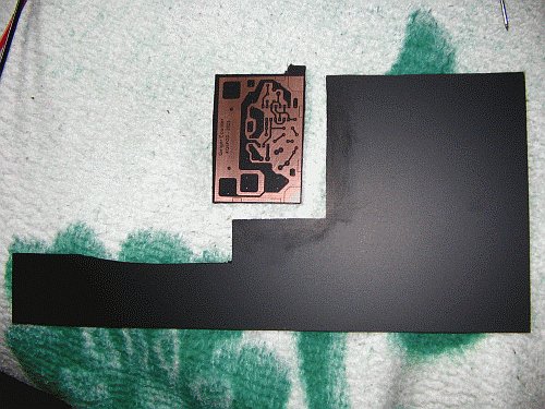
To cut PCB material, I
simply use a hand saw with a fine-toothed metal-cutting blade. I place
a rag over the board while holding it, so that I don't damage the
paint. I left a small margin on all sides, so that I can later sand the
PCB to the precise final size, with good finish of the edges.
There
are some smear marks on the remaining raw board, which happened during
cleaning with alcohol. They are of no consequence, and won't impair the
quality of future PCBs made with that board.
Etching
 Before
I etch a PCB, I warm up the bottle of etchant by placing it in hot
water for half an hour, in the kitchen sink. I let it warm up while I
cut out the board, and store the laser engraver. Then I renew the hot
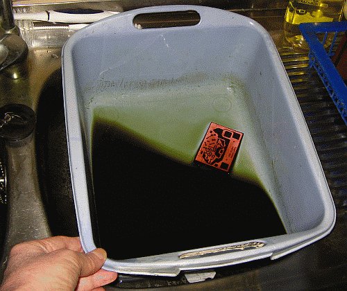
water in the sink, and float a plastic tray in it. The PCB goes
in it, copper side up, and warm etchant is poured into the tray. The
hot water keeps the etchant warm, and the floating tray can very easily
and comfortably be rocked in all directions, to keep the
etchant in constant agitation. I do this rocking by hand, since I'm a
patient guy, but more impatient people might want to build a
contraption with a motor to agitate the etchant. Agitation is very
important! Without it, the etchant would undercut the narrow traces
well before finishing the removal of copper from the larger
clear
areas. This effect is due to local exhaustion of the etchant in those
places where copper is more abundant.
Before
I etch a PCB, I warm up the bottle of etchant by placing it in hot
water for half an hour, in the kitchen sink. I let it warm up while I
cut out the board, and store the laser engraver. Then I renew the hot
water in the sink, and float a plastic tray in it. The PCB goes
in it, copper side up, and warm etchant is poured into the tray. The
hot water keeps the etchant warm, and the floating tray can very easily
and comfortably be rocked in all directions, to keep the
etchant in constant agitation. I do this rocking by hand, since I'm a
patient guy, but more impatient people might want to build a
contraption with a motor to agitate the etchant. Agitation is very
important! Without it, the etchant would undercut the narrow traces
well before finishing the removal of copper from the larger
clear
areas. This effect is due to local exhaustion of the etchant in those
places where copper is more abundant.
To etch double-sided
boards, I first wrap the board in a few loops of plastic-insulated
wire. So the board is inside a kind of cage, that protects both
surfaces from contact with the bottom of the tray. The wire touches the
board only at the edges, at the end of the wire is a convenient place
to grab with bare fingers and lift the board out of the juice to look
at its underside.
 This
photo shows the board near the end of the etching process. Even with
vigorous agitation, the edges of the PCB complete first, and any large
clear areas away from the edges are the last to complete. The stronger
the agitation is, the less pronounced this unevenness is.
This
photo shows the board near the end of the etching process. Even with
vigorous agitation, the edges of the PCB complete first, and any large
clear areas away from the edges are the last to complete. The stronger
the agitation is, the less pronounced this unevenness is.
The total time required for etching a 35µm copper board is
about 10 minutes.
There are a lot of different copper etching solutions. Since acrylic
paint is pretty good at resisting chemicals, any of those etchants should work
fine with this method. Over the years I have used five or six different
etchants, but at the end I came back to the eternally renewable
chloride mix. This juice starts life as a simple
solution of ferric
chloride (AKA iron perchloride) in water, with about 300 grams per liter
being a decent strength. It can be used without further ado, but will
eventually become exhausted. It's here where maintenance of the
solution enters the scene.
When
iron perchloride (FeCl3) dissolves in water, some of the chloride ions
will split up some of the water (H2O), forming some hydrochloric acid
(HCl dissolved in water). This frees up some iron ions, which combine
with the hydroxide ions of the hydrolyzed water, to form iron
hydroxide, Fe(OH)3. This stuff, commonly known as rust, is
poorly
soluble, and will slowly settle in the bottom of the bottle, as a
rust-colored slurry. It's perfectly useless there. It looks as if not
all of the iron perchloride dissolved, but that's not the case. Some
people think that it's copper dust taken off the boards, but that's
also not the case. And what's worse is that when some water
evaporates out of the solution, more rust forms immediately, in very
fine specks, and settles in the pores of any surfaces it finds. So the
solution stains everything it touches, and has earned a bad reputation
for this.
But that doesn't need to be that way! To make good use
of the rust slurry in the bottom of the bottle, all that's needed is
adding some hydrochloric acid! The excess of chloride
ions will
reconvert the rust into iron perchloride. As long as the solution
contains enough hydrochloric acid, no new rust will form, and the
solution will no longer stain anything. It can actually be used to
remove stains it made before adding acid!
As the juice is
used to etch PCBs, iron perchloride (FeCl3) converts to iron-II chloride
(FeCl2), while the free chloride ions convert copper from the PCBs into
copper-I chloride (CuCl). Given an excess of chloride, coming from
hydrochloric acid, and free access to oxygen from the air, the copper-I
chloride will turn into copper perchloride (CuCl2), which is an
excellent etchant by itself!
The bottom line is that this
solution can be stored and used forever, just by letting it breathe
air, and adding some hydrochloric acid whenever it begins to form a
rust slurry in the bottom of the bottle. Over time the copper
perchloride contents will build up, gradually turning your
brown iron perchloride etchant into a green/blue, mostly copper perchloride etchant, but it
will
keep working.
Hydrochloric acid bought in a hardware store,
often called muriatic acid there, has a rather low
concentration,
so that by using this stuff you are adding far more water than
actual hydrochloric acid to your juice. But anyway a lot of water evaporates while
using the warm juice in an open tray, so that roughly
compensates.
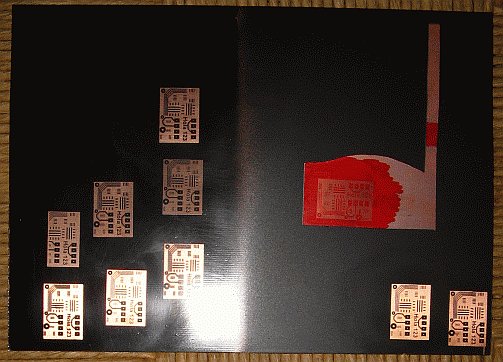
 This
is the fully etched board, after rinsing and drying. There is a small
defect in one of the cutout markings, which I made with 0.2mm wide
traces. Probably I was a bit careless and scratched the paint there. It
doesn't matter. Also some very tiny specks of copper are left in the
area below the text. I didn't see them while etching. Just one more
minute in the etchant would have etched them away, but since they
don't affect the usability of the PCB, I didn't throw it back into the
etchant.
This
is the fully etched board, after rinsing and drying. There is a small
defect in one of the cutout markings, which I made with 0.2mm wide
traces. Probably I was a bit careless and scratched the paint there. It
doesn't matter. Also some very tiny specks of copper are left in the
area below the text. I didn't see them while etching. Just one more
minute in the etchant would have etched them away, but since they
don't affect the usability of the PCB, I didn't throw it back into the
etchant.
Borders
 To
get the board to the exact size, my method is this: I design the board
in CiDess, defining the work area as the size of the PCB, with
zero margins, and I design
the board so that the borders of it are copper-free. That way at the
end of the etching process I get the board in the photo above, with the
PCB edge clearly marked by the transition from copper to no-copper. To
get
the board to the exact dimensions, I simply have to sand away all the
margins that still have copper. This is quick when using a belt
sander. It can also be done by placing a sheet of sandpaper on the
bench, business side up, and rubbing the board on it. It's quite a bit
slower
but also works well.
To
get the board to the exact size, my method is this: I design the board
in CiDess, defining the work area as the size of the PCB, with
zero margins, and I design
the board so that the borders of it are copper-free. That way at the
end of the etching process I get the board in the photo above, with the
PCB edge clearly marked by the transition from copper to no-copper. To
get
the board to the exact dimensions, I simply have to sand away all the
margins that still have copper. This is quick when using a belt
sander. It can also be done by placing a sheet of sandpaper on the
bench, business side up, and rubbing the board on it. It's quite a bit
slower
but also works well.
The Geiger counter board needed some cutouts, to
fit my project box. I marked those cutouts with 10 mil traces in the
design, but then I was lazy and made those cutouts with a handheld
Dremel tool, using a cutting disk and then a grinding stone. Since I'm
now an old guy, using half a dozen different glasses and still not seeing
well close-up, my cutouts came out horrible! But it doesn't
affect usability, so I called it a success anyway. The board does fit
the box, after all...
Paint removal, and surface protection
 Since
I don't like to solder through stubborn stinky black paint, I prefer removing
the paint after etching the board. Sources say that acrylic paint
dissolves readily in acetone, but my acetone bottle was empty... and I
live a long drive away from the closest town, so sprinting out to buy
some acetone was not a good option. I looked around what I had. Alcohol
doesn't attack this paint. I tried lacquer thinner, with no results. I
also tried acrylic thinner, which is almost the same stuff, and it
didn't work either. That's strange, because both are supposed to contain quite
a lot of acetone, in addition to various other solvents!
Since
I don't like to solder through stubborn stinky black paint, I prefer removing
the paint after etching the board. Sources say that acrylic paint
dissolves readily in acetone, but my acetone bottle was empty... and I
live a long drive away from the closest town, so sprinting out to buy
some acetone was not a good option. I looked around what I had. Alcohol
doesn't attack this paint. I tried lacquer thinner, with no results. I
also tried acrylic thinner, which is almost the same stuff, and it
didn't work either. That's strange, because both are supposed to contain quite
a lot of acetone, in addition to various other solvents!
Scraping
the paint away is not something I would like to do. It would totally
scratch the copper, and maybe damage some trace.
So I
searched in my memories, and came up with one that tells that when
handling brake fluid one has to be careful to not let it drip on any
painted surface, because it attacks every paint known to mankind.
Bingo! I pilfered a few drops of DOT3 brake fluid out of my car,
spread it on the PCB, waited a while, and then simply wiped the brake
fluid and the paint off!
Leaving the copper unprotected will
cause it to tarnish over time. If the board won't be used in a harsh
environment, this isn't a problem, but PCBs look nicer if they stay
shiny even after many years. For that to happen, the copper needs to be
protected from the ambient. There are several ways to do it. Some
people love to apply a solder resist mask, but that involves as many
steps as making the PCB proper, so I think it's total overkill. Solder
masks make a lot of sense when an automatic soldering process is used,
that relies on the solder mask to make the solder go only where it has to.
But it makes almost no sense at all for hand soldering, which is what
homebrewers normally do! In fact a solder mask is a nuisance when it
comes to making modifications.
Other people use immersion tin
plating. That's indeed an excellent thing to do, being quick, providing
acceptable protection, long-time solderability, and looking good. The problem
is that a suitable tin plating solution is needed, and I haven't been
able to get any. Due to postal regulations... you know. Absolutely no
chemicals can be shipped. And to make my own, I need thiourea,
among other substances. I can get or make everything else required, but
not thiourea. So, no immersion tin plating for me.
Some
people painstakingly tin their boards with solder and a soldering iron,
or cover it with paste solder and then heat it up. That makes a thick,
good protective layer, but doesn't look very good.
So I resort
to varnishes. In the good old times, I sprayed Kontakt Chemie SK-10
solderable varnish on my boards, and that worked fine. Currently I use
a flux spray, made by an Argentinian company, but it stays somewhat
sticky, so it's not very nice. In between I have used shellac, very diluted
in alcohol, and brushed on. It works fine, but stinks while soldering.
A
good protection method for boards that will be used in harsh environments is to
leave the copper naked at first, assemble the circuit, test it, then
clean the board with alcohol, and spray polyurethane varnish over
everything, copper and solder joints. A board protected in that way can
be used in a harsh environment aboard a yacht for many years, and
remain perfectly good and shiny! But soldering through the polyurethane varnish,
in case repairs are needed, is dirty and stinky.
For my Geiger counter board I used the Argentinian flux lacquer spray.
Drilling
Some
people shudder when even just thinking about manually drilling a few
hundred little holes at precise locations on a large PCB. And indeed it
is somewhat of a nightmare, when the drill bit dances all around the
area and then makes a hole right between
two pads, or when the drill bit breaks, the spare one also breaks, and
then the spare of the spare breaks too, and you are left without drill
bits.
 But
drilling PCBs is easy and quick, when using the correct tools, and
doing it the right way. The first point is using PCB software that
makes guide holes of the right size in each pad. These
little holes etched into the copper will guide the drill bit, so
that
every hole ends up quite precisely where it should, requiring little
effort. And the best drill bit to be used for the small holes in PCBs
is actually not a drill bit, but a dental bur! While drill bits
are long and of constant
diameter, making them break very easily, dental burs
are short
and have a conical shaft. I have never managed to break one!
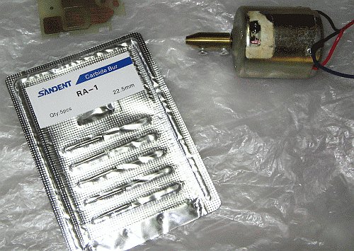
But
drilling PCBs is easy and quick, when using the correct tools, and
doing it the right way. The first point is using PCB software that
makes guide holes of the right size in each pad. These
little holes etched into the copper will guide the drill bit, so
that
every hole ends up quite precisely where it should, requiring little
effort. And the best drill bit to be used for the small holes in PCBs
is actually not a drill bit, but a dental bur! While drill bits
are long and of constant
diameter, making them break very easily, dental burs
are short
and have a conical shaft. I have never managed to break one!
Dental
burs can be mounted in various sorts of motors and chucks. Inexpensive
handheld drill motors are available, but I used the motor of an old
8-track tape player, and made a very basic coupling piece on my lathe.
It uses set screws, making it very unbalanced, so my drill vibrates
quite a bit, but even so it works well enough. Some day I will make a
better coupler, but this one has done the job for many years.
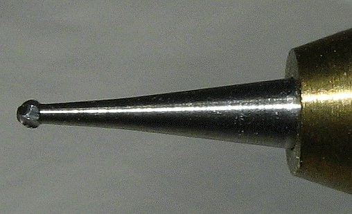 Dental
burs come in many types. For PCB drilling, we need tungsten carbide
burs, not any diamond burs. The carbide ones cut cleanly, while the
diamond ones just abrade, and generate lots of dust and heat.
Dental
burs come in many types. For PCB drilling, we need tungsten carbide
burs, not any diamond burs. The carbide ones cut cleanly, while the
diamond ones just abrade, and generate lots of dust and heat.
The
ones I'm currently using are of the round type. They work quite well, but
years ago I had others that were almost round, but forming a slight
tip, which helped them drill straighter holes. If I get a choice, I
would prefer that slightly pointy round shape over the fully round one
shown here.
The proper size for most PCB holes is 0.8mm. So
that's the bur size I use. I have the software put
0.6mm guide holes into all pads, and then drill all holes with my 0.8mm dental burs.
To do that, I hold the board in one hand, at a 45° angle to the
desktop, and hold the drill motor in my other hand, with the axis at a
right angle to the board. That gives me a good view of the drilling
area, and allows me to rest both wrists and the board edge on the desk. This
allows easy and quick positioning. I just place the bur somewhere on
the guide hole, holding the motor loosely, and the bur will self-center
in the guide hole.
I power the motor from a lab power supply,
adjusting the voltage to get the speed that seems to work best. It's
probably something around 2000 RPM.
After
drilling all holes to 0.8mm in this way, I use common drill bits of
various sizes, in a common little handheld drill, to enlarge the few
holes that need to be larger. In my Geiger counter PCB, there were only
two holes that needed to be enlarged to 1mm, for a 1A diode, and two
bolt holes that needed enlargement to 3mm.
There are also four
slots on this board, to mount a little transformer. These slots are
easily made by using the dental bur as a router, cutting sideways. In
this case I had etched just one guide hole per slot, so I drilled two more
holes per slot, in a row, and then joined each group of three holes
into a slit, by this sideways cutting. Some of my slots ended up
slightly crooked. To get even better slots, the way to go is to place
several pads in the design, very close together, like 1mm to 1/20th inch between
centers, then drill all those holes using the guide holes, and then
join them into slots by sideways milling. It's actually easier to do
than it sounds!
Resolution limitations
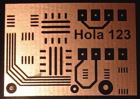 The
Geiger counter board is a very coarse design, using only through-hole
parts, and using 1mm wide traces. Most modern circuitry needs much
finer features. To optimize my process, and see what it can deliver, I
designed this very small 25×18mm test board. It has one DIP-8 footprint
and three through-hole pads, plus horizontal and vertical footprints
for SOIC-8, MSOP-8 and micro-SOIC-8 ICs. The latter has a pin pitch of
0.5mm, compared to 0.65mm for MSOP, 1.27mm for SOIC, and 2.54mm for DIP outlines.
The
traces at the DIP footprint are 20 mils wide, about 0.5mm, while the
four traces
forming a bus with 45° bends are 10 mils wide, about 0.25mm,
with a nominal pitch of 0.5mm between centers.
You can see that everything came out sharp and good, and should etch
without trouble. This means that the laser-engraver-made PCBs are
plenty good enough to use with even the smallest components I have ever
used. Also the dimensional accuracy is very good, better than with any
of the printers I have used to make photo masks.
But
there is still room for minor improvement. If you look closely, you
will notice that the fine traces are not all of identical width and
spacing - but they should! What happens there is quantization
errors. CiDess software works at a resolution of 1200 DPI,
which is 0.021167mm. But track widths are set in mils (1000 DPI, steps
of 0.0254mm). And the laser engraver
works directly in metric units, and has a resolution of 80 steps per
mm, which
is 0.0125mm. All this causes quantization errors. If I draw a
10 mil trace, which is the narrowest CiDess will do, this should of course be
0.01 inch wide, which is 0.254mm. At the 1200 DPI resolution of the
program, this trace will be exactly 12 pixels wide, which is fine. But that would be 20.32
engraver resolution steps! The engraver can in principle draw that
track either as 20 lines or as 21 lines, giving it a width of
either 0.25 or 0.2625mm. Which one, would depend on where that trace is
located, relative to the engraver's steps.
But it won't actually burn 20 or 21 lines! What it does, instead,
is trying to follow the instructions it gets from CiDess. And those
tell it to move in steps of 0.021167mm, and draw the trace in 12 lines
of that width. The engraver will then round each of those 12 line
positions to the nearest positions it can move to, which are in steps
of 0.0125mm. Since one CiDess step is 1.69333 engraver steps, the
engraver will burn 12 laser lines, but some of them will be separated
by 0.0125mm between centers, and the others by 0.025mm between
centers. The end effect is the same: Some traces will end up
0.0125mm wider than some others.
The problem becomes worse with the metric spacing of those micro-SOIC
ICs. Their 0.5mm pin pitch is 23.62204724 pixels at 1200 DPI,
an irrational number. So CiDess will place some of those traces at a
distance of 23 pixels between centers, or 0.48683333mm, and the others
at 24 pixels between centers, or 0.508mm. When the engraver gets these
instructions, it will round them to its own step size: It can place
things at distances of 0.475mm, 0.4875mm, 0.5mm, and 0.5125mm, and will
use any of these values, depending on what it's getting from CiDess,
and where each pair of traces is on its grid. This is a 7.5% tolerance
band! The irritating point is that if the PCB software would work in
metric units, the engraver could place all these tracks at the
exact right locations.
Older electronic parts came in inch-based dimensions, and so it's
logical that PCB software works in inches. But modern parts tend to be
mostly metric, so new PCB software should work in a metric grid.
Particularly because modern parts are far smaller than old ones,
requiring more accuracy.
To
solve the quantization problem, it's necessary to use a consistent
resolution in
the whole process, from PCB design to engraving. Since my laser
engraver works in steps of 0.0125mm,
the PCB software should also work in that grid size, and should output
raster images at that same pixel pitch. This would still cause
quantization errors with component dimensions that are in inches, or
otherwise irrationally related to 0.0125mm, but since this would be
just one step of quantization instead of two, the error would be
smaller, at most as large as one half scan line, not as two
scan
lines like it is now!
PCB software that works in vectors rather than in pixels doesn't
have this problem. But it has another problem in its place: Rounding
errors, that makes traces not meet cleanly, when they should.
Maybe some day I will write my own PCB design software. But for now,
CiDess is good enough as it is.
It should be mentioned that all these step sizes I'm writing about
are actually smaller than the laser spot. So it's a bit of hair
splitting to care about these matters, but I do, because the
quantization errors can be clearly seen when making very fine PCBs!
Even with a 0.08mm wide laser spot, it makes a visible difference if
it's placed, say, 0.025mm shifted.
Anyway the end result is quite good. And if
you compare this photo to the one shown above in the section about
engraver configuration, you will see a big quality improvement between
the two. It's due to two changes: Increasing the laser PWM frequency,
and
optimizing the laser dot size compensation settings in my G-code
conversion program's configuration file.
Note that there
is a smear and some light scratches on the copper. I didn't even clean
it for these tests... Also note that in several photos on this page the
copper looks rough. In fact it's pretty smooth, but looks rough when
using almost frontal lighting, combined with the sharpening applied by
the camera. And due to the low resolution at which I'm publishing these
photos, and the sharpening, lines that are not perfectly vertical nor
horizontal appear with a staircase distortion. They are not like that on the actual boards!
What I cannot do
What
I still cannot do at home is through-hole plating. It would be useful
to have that capability, but it's not essential. Most of my PCBs are
single-sided anyway! I love the marvelous simplicity, practicality and
logic of having all components on one side of a board, and all
connections on the other side, with everything in plain view and easily
reachable. Even quite complex circuits can be built on single-sided
boards, just by making a clever layout, and maybe by cheating a little
where necessary, for example by leaving the leads of a resistor a
little longer to jump over an obnoxious track that doesn't want to be
shifted out of the way.
When I do make double-sided PCBs, I solder them on both sides,
and I design them so that no pins that are inaccessible under a
component needs to be soldered on the top side, and
that mostly the
pins of through-hole components that are accessible on the top side do
double duty as vias. If I really
need a via where there is no suitable component, I simply solder a piece of wire through a hole. In RF
circuits I join the top groundplane to the bottom one, if
needed,
by means of copper sheet strips soldered around all edges, plus wire
vias in all relevant locations. Plated-through holes would certainly make things
easier, but are not essential.
I would also like to get hold of some thiourea, to make immersion tin
plating solution.
Instead solder masks and component overlays are essentially useless for
homebrewing, so I don't miss them.
Back to homo ludens
electronicus.